
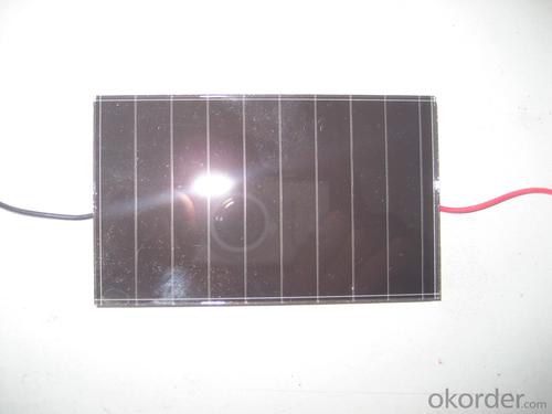
Thin Silicon Wafer Solar Cell - Amorphous Silicon Dice Specification 5
- Ref Price:
-

- Loading Port:
- China Main Port
- Payment Terms:
- TT OR LC
- Min Order Qty:
- -
- Supply Capability:
- -
OKorder Service Pledge
OKorder Financial Service
You Might Also Like


Pv modules at present, the mainstream products are still in silicon as the main raw materials, only in terms of silicon raw material consumption, production 1 mw of crystalline silicon solar cell, need 10 to 12 tons of high purity silicon, but if use the same silicon materials used to produce thin film amorphous silicon solar cell can produce more than 200 mw.
From the perspective of energy consumption, amorphous silicon solar battery only 1-1.5 years of energy recovery period, more embodies its contribution to energy saving in the manufacturing process.
Component occupies a high proportion of costs in a photovoltaic system, the component prices directly affect the system cost, and thus affect the cost of photovoltaic power generation. Calculated at the current price of components, the same money, buy amorphous silicon products, you can get more close to 30% of the power components.
2, more power
For the same power of solar cell array, amorphous silicon solar cell is about 10% more than monocrystalline silicon, polycrystalline silicon battery power. This has been the Uni - Solar System LLC, Energy Photovoltaic Corp., Japan's Kaneka Corp., the Netherlands Energy research institute, and other organizations and experts confirmed that the Photovoltaic industry.
In sunny, that is to say, under the high temperature, amorphous silicon solar cell components can show more excellent power performance.
3, better low light response
Due to the characteristics of amorphous silicon atoms are arranged disorderly, the electron transition no longer comply with the restriction of traditional \"selection rule\", as a result, its light absorption characteristics and there are big differences monocrystalline silicon material. Amorphous silicon and monocrystalline silicon material absorption curve as shown
, amorphous silicon absorption curve has obvious three sections (A, B, C). Area A corresponding electronic transition between localized states, such as the gap state near Fermi level and to the tail state transition, the absorption coefficient is small, about 1-10 cm - 1, for this is absorbing; B area absorption coefficient with the increase of the photon energy index rose, it corresponds to the electrons from the valence band edge extension state to the conduction band localized state transition, as well as the localized electrons from the valence band tail states guide for edge extension state transition, the region's energy range is usually only about half of the electron volts, but absorption coefficient across two or three orders of magnitude, usually up to 104 cm - 1; Area C corresponds to the electrons from the valence band to the conduction band internal internal transition, the absorption coefficient is bigger, often in more than 104 cm - 1. After two absorption area is crystalline silicon eigen absorption area.
Can be seen in the figure, the intersection of two curves about 1.8 ev. It is important to note that in the visible light range (1.7 to 3.0 ev), the absorption coefficient of amorphous silicon material is almost an order of magnitude larger than the single crystal silicon. That is to say, in the morning the first part of the sun is not too strong, the second half, and it's cloudy in the afternoon under the condition of low light intensity, long wave is greater, the amorphous silicon material still has a large absorption coefficient. Again considering the amorphous silicon band gap is larger, the reverse saturation current I0 is smaller. And as mentioned the amorphous silicon battery the characteristics I - V characteristic curve of the amorphous silicon solar cell both in theory and in practical use in low light intensity has good adaptation.
• I - V characteristics of amorphous silicon cells after more than a Vm with the voltage drop slowly
In order to be convenient, we draw the I - V characteristics of two kinds of batteries on the same picture. Crystalline silicon and amorphous silicon battery I - V characteristics of general shape as shown
we see from the picture, two kinds of cells in the curve changes after exceed the maximum output power point gap is bigger. Output current of crystalline silicon cells after exceed the maximum output power point will soon fall to zero, curve steep; Rather than crystalline silicon cells output current after a long distance to fall to zero, the curve is relatively flat. Two kinds of battery Vm equivalent to about 83% of its open circuit voltage and 83% respectively.
when light intensity gradually become hour, short circuit current and open circuit voltage of solar battery will be stronger. Short circuit current decreases faster, of course, open circuit voltage decrease more slowly.
do in battery solar cell array under the condition of load, when the sun battery array of effective output voltage less than the terminal voltage of battery, battery cannot be recharged. When the light intensity gradually become hour, crystal silicon battery charging does not meet the conditions, and amorphous silicon due to the larger voltage difference, do not charge until the light is very dark, effectively increase the use of sunlight time. So, amorphous silicon cells to produce more electricity than the crystalline silicon.
4, more excellent high temperature performance
High in the outdoor environment temperature, amorphous silicon solar cell performance change, depends on the temperature, spectrum, as well as other related factors. But what is certain is: amorphous silicon than monocrystalline silicon or polycrystalline silicon are less likely to be affected by temperature.
Amorphous silicon solar cells than monocrystalline silicon, polycrystalline silicon cells have relatively small temperature coefficient of amorphous silicon solar cell output power best Pm temperature coefficient is about 0.19%, and monocrystalline silicon, polycrystalline silicon cells best output power Pm temperature coefficient is about 0.5%, when the battery work at higher temperatures, the two batteries will be a drop in the Pm, but the decline is different. They can be calculated using the following formula.
- Q: What is the harm of silicon chip into the fingers?
- The silicon rod into silicon wafer after printed, someone with bare hands touched the wafer, because the chemical composition of the finger is very complex, in the cleaning process is not removed, causing subsequent corrosion is not uniform, the more to the more obvious after section
- Q: How does the efficiency of a solar silicon wafer vary with different angles of sunlight?
- The efficiency of a solar silicon wafer varies with different angles of sunlight. The ideal angle for maximum efficiency is when the sunlight is perpendicular to the surface of the wafer. As the angle deviates from perpendicular, the efficiency decreases. This is because the photons have to travel a longer distance through the silicon material, resulting in higher chances of absorption and scattering, thus reducing the overall conversion of sunlight into electricity.
- Q: What is the purpose of a solar silicon wafer in a solar cell?
- The purpose of a solar silicon wafer in a solar cell is to act as the main building block for converting sunlight into electricity. The wafer is made from highly purified silicon and plays a crucial role in capturing and absorbing sunlight, generating an electric current through the photovoltaic effect.
- Q: How is a microinverter integrated into a solar silicon wafer?
- A microinverter is not directly integrated into a solar silicon wafer. Instead, it is typically connected to the solar panels after the silicon wafer has been manufactured and made into a solar cell. The microinverter is then installed on the back of each individual solar panel, allowing for the conversion of the DC (direct current) power generated by the solar panel into AC (alternating current) power that can be used by the electrical grid or household appliances.
- Q: How is an encapsulant applied to a solar silicon wafer?
- An encapsulant is typically applied to a solar silicon wafer by using a process called lamination. In this process, a layer of encapsulant material, usually ethylene-vinyl acetate (EVA), is placed between the silicon wafer and a top layer of glass. The wafer, encapsulant, and glass are then sandwiched together and subjected to heat and pressure. This causes the encapsulant to melt and flow, adhering to the wafer and creating a protective layer that encapsulates the solar cells.
- Q: Can solar silicon wafers be used in wearable fashion accessories?
- Yes, solar silicon wafers can be used in wearable fashion accessories. They can be integrated into various accessories like jewelry, clothing, or accessories such as bags and hats to harness solar energy for charging devices or powering other functionalities.
- Q: How do solar silicon wafers handle temperature variations?
- Solar silicon wafers are designed to handle temperature variations quite well. This is because they are typically made from high-quality materials that have been carefully engineered to withstand extreme temperatures. The wafers have a low coefficient of thermal expansion, meaning they expand and contract minimally with temperature changes. This helps to prevent cracking or damage to the wafers. Additionally, solar cells are often encapsulated in protective materials that provide insulation and help regulate temperature, further enhancing their ability to handle temperature variations.
- Q: How are solar silicon wafers affected by surface passivation techniques?
- Surface passivation techniques have a significant impact on solar silicon wafers. These techniques aim to reduce the recombination of charge carriers at the surface of the wafers, thereby increasing their efficiency in converting sunlight into electricity. Passivation helps to minimize surface defects and traps, ensuring better electron-hole separation and reducing the loss of electrical energy. Overall, surface passivation techniques play a crucial role in enhancing the performance and overall effectiveness of solar silicon wafers.
- Q: How is an interconnect created in a solar silicon wafer?
- An interconnect in a solar silicon wafer is created by using a conductive material, typically a metal, to connect the different solar cells within the wafer. This is done by applying the conductive material in a pattern that allows for the flow of electrical current between the cells, enabling them to work together and generate electricity efficiently.
- Q: How do solar silicon wafers handle extreme temperatures?
- Solar silicon wafers are designed to handle extreme temperatures quite effectively. They are typically made of high-purity crystalline silicon, which has excellent thermal stability and can withstand both hot and cold conditions. Additionally, the wafers are often coated with anti-reflective and anti-corrosive materials that further enhance their resistance to temperature variations. This allows solar silicon wafers to maintain their efficiency and structural integrity even in extreme temperature environments.
Send your message to us
Thin Silicon Wafer Solar Cell - Amorphous Silicon Dice Specification 5
- Ref Price:
-
- Loading Port:
- China Main Port
- Payment Terms:
- TT OR LC
- Min Order Qty:
- -
- Supply Capability:
- -
OKorder Service Pledge
OKorder Financial Service
Similar products


Hot products


Hot Searches
Related keywords

