
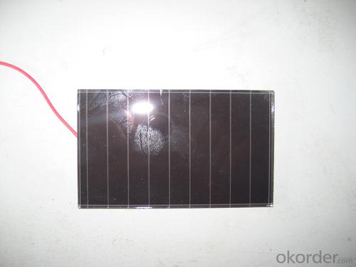
Solar Mono Silicon Wafer Amorphous Silicon Dice Specification 2
- Ref Price:
-

- Loading Port:
- China Main Port
- Payment Terms:
- TT OR LC
- Min Order Qty:
- -
- Supply Capability:
- -
OKorder Service Pledge
OKorder Financial Service
You Might Also Like


Pv modules at present, the mainstream products are still in silicon as the main raw materials, only in terms of silicon raw material consumption, production 1 mw of crystalline silicon solar cell, need 10 to 12 tons of high purity silicon, but if use the same silicon materials used to produce thin film amorphous silicon solar cell can produce more than 200 mw.
From the perspective of energy consumption, amorphous silicon solar battery only 1-1.5 years of energy recovery period, more embodies its contribution to energy saving in the manufacturing process.
Component occupies a high proportion of costs in a photovoltaic system, the component prices directly affect the system cost, and thus affect the cost of photovoltaic power generation. Calculated at the current price of components, the same money, buy amorphous silicon products, you can get more close to 30% of the power components.
2, more power
For the same power of solar cell array, amorphous silicon solar cell is about 10% more than monocrystalline silicon, polycrystalline silicon battery power. This has been the Uni - Solar System LLC, Energy Photovoltaic Corp., Japan's Kaneka Corp., the Netherlands Energy research institute, and other organizations and experts confirmed that the Photovoltaic industry.
In sunny, that is to say, under the high temperature, amorphous silicon solar cell components can show more excellent power performance.
3, better low light response
Due to the characteristics of amorphous silicon atoms are arranged disorderly, the electron transition no longer comply with the restriction of traditional \"selection rule\", as a result, its light absorption characteristics and there are big differences monocrystalline silicon material. Amorphous silicon and monocrystalline silicon material absorption curve as shown
, amorphous silicon absorption curve has obvious three sections (A, B, C). Area A corresponding electronic transition between localized states, such as the gap state near Fermi level and to the tail state transition, the absorption coefficient is small, about 1-10 cm - 1, for this is absorbing; B area absorption coefficient with the increase of the photon energy index rose, it corresponds to the electrons from the valence band edge extension state to the conduction band localized state transition, as well as the localized electrons from the valence band tail states guide for edge extension state transition, the region's energy range is usually only about half of the electron volts, but absorption coefficient across two or three orders of magnitude, usually up to 104 cm - 1; Area C corresponds to the electrons from the valence band to the conduction band internal internal transition, the absorption coefficient is bigger, often in more than 104 cm - 1. After two absorption area is crystalline silicon eigen absorption area.
Can be seen in the figure, the intersection of two curves about 1.8 ev. It is important to note that in the visible light range (1.7 to 3.0 ev), the absorption coefficient of amorphous silicon material is almost an order of magnitude larger than the single crystal silicon. That is to say, in the morning the first part of the sun is not too strong, the second half, and it's cloudy in the afternoon under the condition of low light intensity, long wave is greater, the amorphous silicon material still has a large absorption coefficient. Again considering the amorphous silicon band gap is larger, the reverse saturation current I0 is smaller. And as mentioned the amorphous silicon battery the characteristics I - V characteristic curve of the amorphous silicon solar cell both in theory and in practical use in low light intensity has good adaptation.
• I - V characteristics of amorphous silicon cells after more than a Vm with the voltage drop slowly
In order to be convenient, we draw the I - V characteristics of two kinds of batteries on the same picture. Crystalline silicon and amorphous silicon battery I - V characteristics of general shape as shown
we see from the picture, two kinds of cells in the curve changes after exceed the maximum output power point gap is bigger. Output current of crystalline silicon cells after exceed the maximum output power point will soon fall to zero, curve steep; Rather than crystalline silicon cells output current after a long distance to fall to zero, the curve is relatively flat. Two kinds of battery Vm equivalent to about 83% of its open circuit voltage and 83% respectively.
when light intensity gradually become hour, short circuit current and open circuit voltage of solar battery will be stronger. Short circuit current decreases faster, of course, open circuit voltage decrease more slowly.
do in battery solar cell array under the condition of load, when the sun battery array of effective output voltage less than the terminal voltage of battery, battery cannot be recharged. When the light intensity gradually become hour, crystal silicon battery charging does not meet the conditions, and amorphous silicon due to the larger voltage difference, do not charge until the light is very dark, effectively increase the use of sunlight time. So, amorphous silicon cells to produce more electricity than the crystalline silicon.
4, more excellent high temperature performance
High in the outdoor environment temperature, amorphous silicon solar cell performance change, depends on the temperature, spectrum, as well as other related factors. But what is certain is: amorphous silicon than monocrystalline silicon or polycrystalline silicon are less likely to be affected by temperature.
Amorphous silicon solar cells than monocrystalline silicon, polycrystalline silicon cells have relatively small temperature coefficient of amorphous silicon solar cell output power best Pm temperature coefficient is about 0.19%, and monocrystalline silicon, polycrystalline silicon cells best output power Pm temperature coefficient is about 0.5%, when the battery work at higher temperatures, the two batteries will be a drop in the Pm, but the decline is different. They can be calculated using the following formula.
- Q: What is the effect of temperature on the efficiency of a solar silicon wafer?
- The efficiency of a solar silicon wafer is directly influenced by temperature. As temperature increases, the efficiency of the wafer decreases. This is because the electrical characteristics of the silicon material change with temperature, leading to a decrease in the conversion of sunlight into electricity. Therefore, it is crucial to maintain optimal temperature conditions for a solar silicon wafer to maximize its efficiency and overall performance.
- Q: What is the role of surface recombination on solar silicon wafers?
- The role of surface recombination on solar silicon wafers is to reduce the efficiency of the solar cells. Surface recombination refers to the loss of charge carriers (electrons and holes) at the surface of the silicon wafer, which can significantly limit the performance of the solar cells. By reducing the surface recombination, the efficiency of the solar cells can be improved, leading to higher power output and better overall performance of the photovoltaic system.
- Q: How do solar silicon wafers perform in extreme weather conditions?
- Solar silicon wafers are designed to withstand extreme weather conditions. They are typically made with durable materials that can resist temperature fluctuations, high winds, and heavy rain. Additionally, they undergo thorough testing to ensure their performance and reliability in challenging environments. However, extreme weather events such as hailstorms or hurricanes can still cause damage to the wafers, but this is relatively rare. Overall, solar silicon wafers are built to endure and continue generating electricity even in harsh weather conditions.
- Q: What are the different materials used for backsheets in solar silicon wafers?
- The different materials commonly used for backsheets in solar silicon wafers include polyvinyl fluoride (PVF), polyethylene terephthalate (PET), and ethylene vinyl acetate (EVA).
- Q: What is the expected degradation rate of solar silicon wafers over time?
- The expected degradation rate of solar silicon wafers over time varies depending on several factors including the quality of the materials used, manufacturing processes, environmental conditions, and maintenance practices. However, on average, solar silicon wafers experience a degradation rate of around 0.5-1% per year.
- Q: How are solar silicon wafers affected by temperature-induced stress?
- Solar silicon wafers are affected by temperature-induced stress in several ways. Firstly, as the temperature increases, the thermal expansion of the silicon material causes it to expand, leading to mechanical stress on the wafer. This stress can result in warping or even cracking of the wafer. Secondly, temperature fluctuations can cause differential expansion and contraction across different layers of the wafer, especially if it is a multi-layered structure. This can lead to delamination or detachment of layers, compromising the integrity and performance of the wafer. Thirdly, temperature-induced stress can affect the electrical properties of the silicon material. Increased stress can alter the bandgap and carrier mobility, potentially impacting the efficiency of the solar cell. Overall, it is crucial to carefully manage temperature-induced stress in solar silicon wafers to ensure their structural integrity and optimal performance.
- Q: What is the role of front contacts on solar silicon wafers?
- The role of front contacts on solar silicon wafers is to collect and extract the generated electricity from the solar cells. These contacts are typically made of metal fingers or grids that are placed on the front surface of the solar cell. They enable the flow of current and help in minimizing the resistance and losses, ensuring efficient electricity production from the solar panel.
- Q: What is the effect of surface texturing on solar silicon wafers?
- Surface texturing on solar silicon wafers has a positive effect on their efficiency and performance. It helps to increase light absorption by reducing the reflection of incident sunlight, leading to a higher conversion of solar energy into electricity. Additionally, surface texturing enhances the overall electrical conductivity of the wafers, improving their electrical performance. Thus, surface texturing plays a crucial role in enhancing the efficiency and output of solar cells.
- Q: How do solar silicon wafers perform in high-pollution environments?
- Solar silicon wafers generally perform well in high-pollution environments, thanks to their durable and weather-resistant nature. However, excessive pollution, such as smog or industrial emissions, can potentially reduce their performance by blocking sunlight and creating a layer of grime on the surface. Regular maintenance and cleaning of the solar panels can help mitigate these effects and ensure their optimal performance in such environments.
- Q: Can solar silicon wafers be used in wearable technology?
- Yes, solar silicon wafers can be used in wearable technology. They can be integrated into wearable devices such as smartwatches or fitness trackers to capture and convert solar energy into electrical power, enabling longer battery life or even eliminating the need for external charging.
Send your message to us
Solar Mono Silicon Wafer Amorphous Silicon Dice Specification 2
- Ref Price:
-
- Loading Port:
- China Main Port
- Payment Terms:
- TT OR LC
- Min Order Qty:
- -
- Supply Capability:
- -
OKorder Service Pledge
OKorder Financial Service
Similar products


Hot products


Hot Searches
Related keywords

