
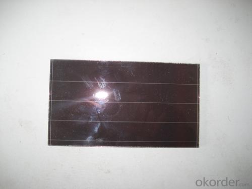
Amorphous Silicon Dice Silicon Wafer Solar Panel Specification 1
- Ref Price:
-

- Loading Port:
- China Main Port
- Payment Terms:
- TT OR LC
- Min Order Qty:
- -
- Supply Capability:
- -
OKorder Service Pledge
OKorder Financial Service
You Might Also Like


Pv modules at present, the mainstream products are still in silicon as the main raw materials, only in terms of silicon raw material consumption, production 1 mw of crystalline silicon solar cell, need 10 to 12 tons of high purity silicon, but if use the same silicon materials used to produce thin film amorphous silicon solar cell can produce more than 200 mw.
From the perspective of energy consumption, amorphous silicon solar battery only 1-1.5 years of energy recovery period, more embodies its contribution to energy saving in the manufacturing process.
Component occupies a high proportion of costs in a photovoltaic system, the component prices directly affect the system cost, and thus affect the cost of photovoltaic power generation. Calculated at the current price of components, the same money, buy amorphous silicon products, you can get more close to 30% of the power components.
2, more power
For the same power of solar cell array, amorphous silicon solar cell is about 10% more than monocrystalline silicon, polycrystalline silicon battery power. This has been the Uni - Solar System LLC, Energy Photovoltaic Corp., Japan's Kaneka Corp., the Netherlands Energy research institute, and other organizations and experts confirmed that the Photovoltaic industry.
In sunny, that is to say, under the high temperature, amorphous silicon solar cell components can show more excellent power performance.
3, better low light response
Due to the characteristics of amorphous silicon atoms are arranged disorderly, the electron transition no longer comply with the restriction of traditional \"selection rule\", as a result, its light absorption characteristics and there are big differences monocrystalline silicon material. Amorphous silicon and monocrystalline silicon material absorption curve as shown
, amorphous silicon absorption curve has obvious three sections (A, B, C). Area A corresponding electronic transition between localized states, such as the gap state near Fermi level and to the tail state transition, the absorption coefficient is small, about 1-10 cm - 1, for this is absorbing; B area absorption coefficient with the increase of the photon energy index rose, it corresponds to the electrons from the valence band edge extension state to the conduction band localized state transition, as well as the localized electrons from the valence band tail states guide for edge extension state transition, the region's energy range is usually only about half of the electron volts, but absorption coefficient across two or three orders of magnitude, usually up to 104 cm - 1; Area C corresponds to the electrons from the valence band to the conduction band internal internal transition, the absorption coefficient is bigger, often in more than 104 cm - 1. After two absorption area is crystalline silicon eigen absorption area.
Can be seen in the figure, the intersection of two curves about 1.8 ev. It is important to note that in the visible light range (1.7 to 3.0 ev), the absorption coefficient of amorphous silicon material is almost an order of magnitude larger than the single crystal silicon. That is to say, in the morning the first part of the sun is not too strong, the second half, and it's cloudy in the afternoon under the condition of low light intensity, long wave is greater, the amorphous silicon material still has a large absorption coefficient. Again considering the amorphous silicon band gap is larger, the reverse saturation current I0 is smaller. And as mentioned the amorphous silicon battery the characteristics I - V characteristic curve of the amorphous silicon solar cell both in theory and in practical use in low light intensity has good adaptation.
• I - V characteristics of amorphous silicon cells after more than a Vm with the voltage drop slowly
In order to be convenient, we draw the I - V characteristics of two kinds of batteries on the same picture. Crystalline silicon and amorphous silicon battery I - V characteristics of general shape as shown
we see from the picture, two kinds of cells in the curve changes after exceed the maximum output power point gap is bigger. Output current of crystalline silicon cells after exceed the maximum output power point will soon fall to zero, curve steep; Rather than crystalline silicon cells output current after a long distance to fall to zero, the curve is relatively flat. Two kinds of battery Vm equivalent to about 83% of its open circuit voltage and 83% respectively.
when light intensity gradually become hour, short circuit current and open circuit voltage of solar battery will be stronger. Short circuit current decreases faster, of course, open circuit voltage decrease more slowly.
do in battery solar cell array under the condition of load, when the sun battery array of effective output voltage less than the terminal voltage of battery, battery cannot be recharged. When the light intensity gradually become hour, crystal silicon battery charging does not meet the conditions, and amorphous silicon due to the larger voltage difference, do not charge until the light is very dark, effectively increase the use of sunlight time. So, amorphous silicon cells to produce more electricity than the crystalline silicon.
4, more excellent high temperature performance
High in the outdoor environment temperature, amorphous silicon solar cell performance change, depends on the temperature, spectrum, as well as other related factors. But what is certain is: amorphous silicon than monocrystalline silicon or polycrystalline silicon are less likely to be affected by temperature.
Amorphous silicon solar cells than monocrystalline silicon, polycrystalline silicon cells have relatively small temperature coefficient of amorphous silicon solar cell output power best Pm temperature coefficient is about 0.19%, and monocrystalline silicon, polycrystalline silicon cells best output power Pm temperature coefficient is about 0.5%, when the battery work at higher temperatures, the two batteries will be a drop in the Pm, but the decline is different. They can be calculated using the following formula.
- Q: Why do you want to make the wafer bigger? The bigger the better, why?
- So the price of a light on the CCD. Because the yield is very low. Astronomical telescopes or military reconnaissance equipment used on the larger size of CCD (such as 4, 8 inches or even 12 inches CCD) is simply astronomical. Looking for a piece of silicon wafer that is close to zero defect is probably a vast project. And the speed of the chip is also affected by the area. The larger the area, the greater the span of the wiring, the greater the frequency of interference and signal
- Q: Ultrasonic cleaning cleaning silicon?
- Yes, but it is said to be the frequency of the 1MHz cleaning machine. Is not an ordinary low-frequency 100K below the frequency of cleaning machine.
- Q: Such as the title, look at some of the information, said the integrated circuit are integrated in silicon, why? Why not integrate on insulator?
- First of all, the general circuit of the insulator, just a carrier, it plays the role of support and insulation. As for the integrated circuit, the bottom layer is called the substrate (generally P type semiconductor), is to participate in the work of integrated circuits. CMOS process, so the Nmos substrate are connected together, are the same substrate.
- Q: Can solar silicon wafers be used in underwater applications?
- Yes, solar silicon wafers can be used in underwater applications. They are designed to be waterproof and can withstand the effects of being submerged in water. However, proper sealing and protection measures need to be in place to prevent any damage or corrosion to the wafers.
- Q: What are the disadvantages of using a solar silicon wafer?
- One of the main disadvantages of using a solar silicon wafer is its high production cost. The manufacturing process of silicon wafers involves complex and energy-intensive procedures, which can significantly increase the overall cost of solar panels. Additionally, silicon wafers are relatively fragile and can be easily damaged during handling and installation, making them less durable compared to other solar technologies. Furthermore, silicon wafers have lower efficiency in converting sunlight into electricity, especially in low-light conditions, which can limit their performance in certain environments.
- Q: What is the purpose of a degradation rate in a solar silicon wafer?
- The purpose of a degradation rate in a solar silicon wafer is to measure and quantify the rate at which the wafer's performance or efficiency deteriorates over time due to various factors such as exposure to sunlight, temperature variations, and environmental conditions. This degradation rate helps in assessing the long-term durability and reliability of the wafer, and enables manufacturers to improve the quality and lifespan of solar panels by identifying potential issues and optimizing their designs and materials.
- Q: What specific steps should be used to clean the wafer? A little more detail
- . Because of the advantages of easy control, low voltage DC drive, rich color after combination, long service life and so on, it is widely used in various engineering, large screen display system. LED can be used as a display, under the control of the computer, display color changes in the video and pictures. LED is a semiconductor capable of converting electrical energy into visible light
- Q: What is the efficiency of a solar panel made from solar silicon wafers?
- The efficiency of a solar panel made from solar silicon wafers can vary depending on various factors such as the quality of the silicon, the manufacturing process, and the technology used. However, on average, solar panels made from silicon wafers can achieve an efficiency of around 15% to 20%.
- Q: Can solar silicon wafers be used in solar-powered security systems?
- Yes, solar silicon wafers can be used in solar-powered security systems. These wafers are commonly used in the production of solar cells, which convert sunlight into electricity. By harnessing solar energy, security systems can operate independently, without relying on grid power or batteries. Solar silicon wafers provide a reliable and sustainable solution for powering security systems, ensuring continuous surveillance even in remote or off-grid locations.
- Q: What is the effect of impurities on the performance of solar silicon wafers?
- Impurities have a detrimental effect on the performance of solar silicon wafers. These impurities can interfere with the flow of electrons, reducing the efficiency of the solar cells. They can also cause defects in the crystal lattice structure, leading to decreased electrical conductivity and overall performance of the wafers. Therefore, minimizing impurities is crucial for maximizing the efficiency and reliability of solar silicon wafers.
Send your message to us
Amorphous Silicon Dice Silicon Wafer Solar Panel Specification 1
- Ref Price:
-
- Loading Port:
- China Main Port
- Payment Terms:
- TT OR LC
- Min Order Qty:
- -
- Supply Capability:
- -
OKorder Service Pledge
OKorder Financial Service
Similar products


Hot products


Hot Searches
Related keywords

