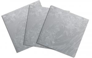


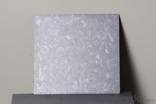
Silicon Wafer in Solar Photovoltaic Cells - Polycrystalline/Multiple Solar Silicon Wafer 156*156
- Ref Price:
-

- Loading Port:
- Shanghai Port
- Payment Terms:
- TT or LC
- Min Order Qty:
- 100 Pieces PCS
- Supply Capability:
- 700MW/Per Year PCS/month
OKorder Service Pledge
Quality Product, Order Online Tracking, Timely Delivery
OKorder Financial Service
Credit Rating, Credit Services, Credit Purchasing
You Might Also Like


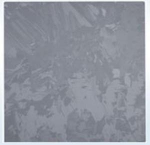
Specifications of Polycrystalline Silicon Wafer
Format : 156 mm × 156 mm ± 0.5 mm
Thickness : 200μm ± 10 μm
| Product name | Poly Wafer |
| Conductive type | P Type |
| Square size wafer (mm) | 156×156±0.5 |
| 219.20±0.5 | |
| Corner (mm)
|
1±0.5、45°±10º |
| 200±20 | |
| Total thickness(um) | ≤40 |
| Resistivity ranges(Ωcm) | 1-3 |
| Doping elements | boron |
| Carbon content(atoms/cc) | ≤8*1017 |
| Oxygen content(atoms/cc) | ≤1*1018 |
| Lifetime(μs) | ≥2 |
| Surface quality | No crack, gap, missing Angle, perforated, window, microcrystalline |
| Warping degrees(μm) | ≤50 |
| Neighbouring vertical degree | 90±0.5° |
| Side damage(mm) | ≤0.5mm(length)×0.3mm(width),(not more than 2 per wafer) |
| Line mark(μm) | ≤15 |
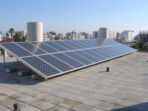
Usage and Applications of Poly Wafers
Poly Solar Wafers mainly used in Poly Solar Cells, with high efficiency and reliable quality. Our Wafer can promise the 25 years life span and have passed PID test.
Packaging & Delivery of Poly Wafers
Carton Box Package and Deliver by air
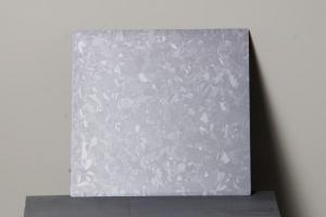
Factory Picture of Poly Wafers

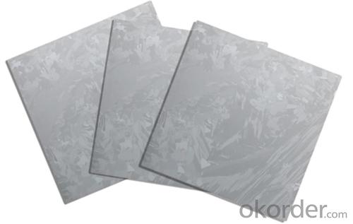
Package Picture of Poly Wafers

- Q: Can solar silicon wafers be used in solar-powered remote sensing devices?
- Yes, solar silicon wafers can be used in solar-powered remote sensing devices. These wafers are commonly used in photovoltaic cells to convert sunlight into electricity, which can then power various electronic devices, including remote sensing devices. Solar silicon wafers provide a reliable and efficient source of renewable energy for such applications.
- Q: What is the global production capacity of solar silicon wafers?
- The global production capacity of solar silicon wafers is estimated to be around 120 GW (gigawatts) per year.
- Q: What is the role of back surface field on solar silicon wafers?
- The role of back surface field on solar silicon wafers is to enhance the efficiency of the solar cell by reducing the recombination of charge carriers at the back surface. It helps to create a strong electric field at the back surface, which prevents the loss of generated electrons and holes. This improved charge collection increases the overall power output of the solar cell.
- Q: How has the technology for solar silicon wafers evolved over time?
- The technology for solar silicon wafers has evolved significantly over time. Initially, the production of silicon wafers was a complex and expensive process, with low efficiency levels. However, advancements in manufacturing techniques and materials have led to the development of more efficient and cost-effective solar silicon wafers. These improvements include the introduction of thin-film solar cells, multicrystalline silicon wafers, and monocrystalline silicon wafers. Additionally, the size of the wafers has increased, allowing for larger solar cells and greater energy generation. Overall, the evolution of solar silicon wafer technology has resulted in increased efficiency, reduced costs, and widespread adoption of solar energy.
- Q: Why not use crystal silicon battery N type silicon, boron diffusion is difficult, or material difficult to do, or the principle of the problem?
- Can use N type silicon chip, the current SUN POWER battery slice, is the use of N type silicon wafer production, conversion efficiency is very high, but the price is not cheap.At present, most of the domestic manufacturers do not have the production of battery N battery pack, it should be a cost problem.
- Q: Why do monocrystalline silicon chamfer? Polysilicon film?
- After the wafer after cutting edge surface with corners burr edge collapse even cracks or other defects, the edge of rough surface. In order to increase the mechanical strength of silicon slice edge surface, reduce particle pollution, will be the edge grinding in a circular arc shape or a trapezoid
- Q: Are solar silicon wafers affected by power outages?
- No, solar silicon wafers are not directly affected by power outages as they are solid-state components that do not rely on continuous power supply. However, during a power outage, the overall solar energy generation system, including inverters and grid connectivity, may be impacted, resulting in a temporary disruption of electricity production from solar panels.
- Q: How is the purity of silicon determined for solar wafers?
- The purity of silicon for solar wafers is determined through various methods, including chemical analysis and spectroscopy techniques. These methods assess the concentration of impurities such as metals, oxygen, and carbon in the silicon material. Additionally, the resistivity of the silicon is measured as an indicator of its purity. This thorough analysis ensures that the silicon used in solar wafers meets the required purity standards for efficient solar cell performance.
- Q: Can solar silicon wafers be used in solar-powered medical devices?
- Yes, solar silicon wafers can be used in solar-powered medical devices. Solar silicon wafers are commonly used in solar panels to convert sunlight into electricity, and this electricity can be utilized to power various medical devices, including those used in remote or off-grid areas. By harnessing solar energy, these devices can operate independently without relying on traditional power sources, making them more sustainable and accessible in diverse healthcare settings.
- Q: What is the role of solar silicon wafers in space exploration?
- Solar silicon wafers play a crucial role in space exploration as they are used to manufacture solar panels that generate electricity from sunlight in space. These panels provide power to spacecraft and satellites, enabling them to function and carry out essential tasks like communication, data collection, and navigation in the harsh space environment. Solar silicon wafers are highly efficient in converting sunlight into electrical energy, making them an integral component in powering various space missions.
Our company is a world class resources and green energy developer, operator and supplier with its engagement in green energy development, integration and operation. We strives to offer highly efficient, eco-friendly, economical and reliable energy solutions through an integrated and diversified energy industrial chain. In adherence to the philosophy of bringing green power to life, the Group stays committed to continuously providing high-quality energy and services for a better living environment. Under approaches of people-oriented, excellence-foremost, value-creation and harmony-pursuant, our Group is determined to become a respected world-class green energy conglomerate.
1. Manufacturer Overview
| Location | |
| Year Established | |
| Annual Output Value | |
| Main Markets | |
| Company Certifications |
2. Manufacturer Certificates
| a) Certification Name | |
| Range | |
| Reference | |
| Validity Period |
3. Manufacturer Capability
| a) Trade Capacity | |
| Nearest Port | |
| Export Percentage | |
| No.of Employees in Trade Department | |
| Language Spoken: | |
| b) Factory Information | |
| Factory Size: | |
| No. of Production Lines | |
| Contract Manufacturing | |
| Product Price Range | |
Send your message to us
Silicon Wafer in Solar Photovoltaic Cells - Polycrystalline/Multiple Solar Silicon Wafer 156*156
- Ref Price:
-
- Loading Port:
- Shanghai Port
- Payment Terms:
- TT or LC
- Min Order Qty:
- 100 Pieces PCS
- Supply Capability:
- 700MW/Per Year PCS/month
OKorder Service Pledge
Quality Product, Order Online Tracking, Timely Delivery
OKorder Financial Service
Credit Rating, Credit Services, Credit Purchasing
Similar products


Hot products


Hot Searches

