
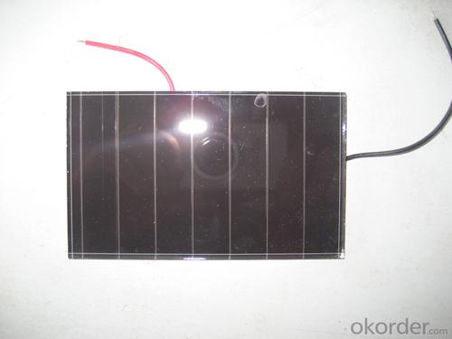
IC Grade Amorphous Silicon Dice Specification 3 Solar Silicon Wafer
- Ref Price:
-

- Loading Port:
- China Main Port
- Payment Terms:
- TT OR LC
- Min Order Qty:
- -
- Supply Capability:
- -
OKorder Service Pledge
OKorder Financial Service
You Might Also Like


Pv modules at present, the mainstream products are still in silicon as the main raw materials, only in terms of silicon raw material consumption, production 1 mw of crystalline silicon solar cell, need 10 to 12 tons of high purity silicon, but if use the same silicon materials used to produce thin film amorphous silicon solar cell can produce more than 200 mw.
From the perspective of energy consumption, amorphous silicon solar battery only 1-1.5 years of energy recovery period, more embodies its contribution to energy saving in the manufacturing process.
Component occupies a high proportion of costs in a photovoltaic system, the component prices directly affect the system cost, and thus affect the cost of photovoltaic power generation. Calculated at the current price of components, the same money, buy amorphous silicon products, you can get more close to 30% of the power components.
2, more power
For the same power of solar cell array, amorphous silicon solar cell is about 10% more than monocrystalline silicon, polycrystalline silicon battery power. This has been the Uni - Solar System LLC, Energy Photovoltaic Corp., Japan's Kaneka Corp., the Netherlands Energy research institute, and other organizations and experts confirmed that the Photovoltaic industry.
In sunny, that is to say, under the high temperature, amorphous silicon solar cell components can show more excellent power performance.
3, better low light response
Due to the characteristics of amorphous silicon atoms are arranged disorderly, the electron transition no longer comply with the restriction of traditional \"selection rule\", as a result, its light absorption characteristics and there are big differences monocrystalline silicon material. Amorphous silicon and monocrystalline silicon material absorption curve as shown
, amorphous silicon absorption curve has obvious three sections (A, B, C). Area A corresponding electronic transition between localized states, such as the gap state near Fermi level and to the tail state transition, the absorption coefficient is small, about 1-10 cm - 1, for this is absorbing; B area absorption coefficient with the increase of the photon energy index rose, it corresponds to the electrons from the valence band edge extension state to the conduction band localized state transition, as well as the localized electrons from the valence band tail states guide for edge extension state transition, the region's energy range is usually only about half of the electron volts, but absorption coefficient across two or three orders of magnitude, usually up to 104 cm - 1; Area C corresponds to the electrons from the valence band to the conduction band internal internal transition, the absorption coefficient is bigger, often in more than 104 cm - 1. After two absorption area is crystalline silicon eigen absorption area.
Can be seen in the figure, the intersection of two curves about 1.8 ev. It is important to note that in the visible light range (1.7 to 3.0 ev), the absorption coefficient of amorphous silicon material is almost an order of magnitude larger than the single crystal silicon. That is to say, in the morning the first part of the sun is not too strong, the second half, and it's cloudy in the afternoon under the condition of low light intensity, long wave is greater, the amorphous silicon material still has a large absorption coefficient. Again considering the amorphous silicon band gap is larger, the reverse saturation current I0 is smaller. And as mentioned the amorphous silicon battery the characteristics I - V characteristic curve of the amorphous silicon solar cell both in theory and in practical use in low light intensity has good adaptation.
• I - V characteristics of amorphous silicon cells after more than a Vm with the voltage drop slowly
In order to be convenient, we draw the I - V characteristics of two kinds of batteries on the same picture. Crystalline silicon and amorphous silicon battery I - V characteristics of general shape as shown
we see from the picture, two kinds of cells in the curve changes after exceed the maximum output power point gap is bigger. Output current of crystalline silicon cells after exceed the maximum output power point will soon fall to zero, curve steep; Rather than crystalline silicon cells output current after a long distance to fall to zero, the curve is relatively flat. Two kinds of battery Vm equivalent to about 83% of its open circuit voltage and 83% respectively.
when light intensity gradually become hour, short circuit current and open circuit voltage of solar battery will be stronger. Short circuit current decreases faster, of course, open circuit voltage decrease more slowly.
do in battery solar cell array under the condition of load, when the sun battery array of effective output voltage less than the terminal voltage of battery, battery cannot be recharged. When the light intensity gradually become hour, crystal silicon battery charging does not meet the conditions, and amorphous silicon due to the larger voltage difference, do not charge until the light is very dark, effectively increase the use of sunlight time. So, amorphous silicon cells to produce more electricity than the crystalline silicon.
4, more excellent high temperature performance
High in the outdoor environment temperature, amorphous silicon solar cell performance change, depends on the temperature, spectrum, as well as other related factors. But what is certain is: amorphous silicon than monocrystalline silicon or polycrystalline silicon are less likely to be affected by temperature.
Amorphous silicon solar cells than monocrystalline silicon, polycrystalline silicon cells have relatively small temperature coefficient of amorphous silicon solar cell output power best Pm temperature coefficient is about 0.19%, and monocrystalline silicon, polycrystalline silicon cells best output power Pm temperature coefficient is about 0.5%, when the battery work at higher temperatures, the two batteries will be a drop in the Pm, but the decline is different. They can be calculated using the following formula.
- Q: How does the electrical conductivity affect the efficiency of a solar silicon wafer?
- The electrical conductivity of a solar silicon wafer directly affects its efficiency as it determines how well the wafer can transport the generated electrical charge. Higher electrical conductivity allows for better electron mobility, resulting in more efficient collection and transport of the generated electricity, thus increasing the overall efficiency of the solar cell.
- Q: How has the technology for solar silicon wafers evolved over time?
- The technology for solar silicon wafers has evolved significantly over time. Initially, silicon wafers were thick and costly to produce. However, advancements in manufacturing techniques have led to the development of thinner wafers, reducing material costs and increasing efficiency. Additionally, the quality of silicon used in wafers has improved, resulting in higher conversion rates and enhanced performance. Moreover, innovative processes like multi-crystalline silicon and monocrystalline silicon have been introduced, further improving the efficiency of solar cells. Overall, the evolution of technology has made solar silicon wafers more affordable, efficient, and accessible, driving the widespread adoption of solar energy.
- Q: 1 megawatts of solar energy need how many wafers
- It depends on whether it is a single crystal or polycrystalline, I only know that polycrystalline is about 3.8 mw.
- Q: What is the role of gettering in solar silicon wafers?
- The role of gettering in solar silicon wafers is to reduce or eliminate impurities and defects that can hinder the performance and efficiency of solar cells. Gettering helps to trap and remove unwanted impurities and contaminants, such as metal impurities and dislocations, from the bulk silicon material. This process ensures that the silicon wafers used in solar cells have a higher purity level, leading to improved electrical conductivity and overall performance of the solar cells.
- Q: What is a good solar wafer testing equipment?
- QCROBOT has been the solar energy as the focus of their products to promote the industry, and has a variety of measurement and control products, for the field of solar energy has launched a variety of measurement and control programs. For example, photovoltaic semiconductor production process control, solar power plant power monitoring system, as well as photovoltaic solar cell volt ampere characteristics test. QCROBOT machine vision system can be used to monitor the shape and size of silicon particles at high temperature. Machine vision can also be used to monitor the quality defects, size measurement, and so on of crystal rods, wafers, panels and components. At present, the QCROBOT vision system and the measurement and control software and hardware platform have been successfully applied to the production and installation process of the solar panel.
- Q: How to detect the surface finish of photovoltaic silicon wafers, what equipment?
- Physical examination of the surface roughness on the line, whether it can be cleaned with chemical or optical
- Q: What is the difference between silicon wafer P111 and P100
- If the crystal is body centered cubic lattice, the crystal orientation through the cube on the diagonal atoms
- Q: How do solar silicon wafers handle temperature variations?
- Solar silicon wafers are designed to handle temperature variations quite well. They have a low coefficient of thermal expansion, which means they can expand and contract without being damaged. The materials used in their construction are highly stable and can withstand a wide range of temperatures, from extreme heat to freezing cold. This resilience allows solar silicon wafers to efficiently convert sunlight into electricity regardless of the surrounding temperature.
- Q: What is the expected degradation rate of a solar silicon wafer over time?
- The expected degradation rate of a solar silicon wafer over time can vary depending on various factors such as the quality of the wafer, the manufacturing process, and the environmental conditions it is exposed to. However, on average, a well-maintained silicon wafer can experience a degradation rate of around 0.5% to 1% per year.
- Q: What factors affect the conversion efficiency of a solar silicon wafer?
- Several factors affect the conversion efficiency of a solar silicon wafer. These include the quality and purity of the silicon material used, the presence of impurities or defects in the wafer, the surface texture and reflectivity, the thickness of the wafer, and the design and performance of the solar cell technology employed. Other external factors such as temperature, humidity, and sunlight intensity also play a role in determining the overall conversion efficiency.
Send your message to us
IC Grade Amorphous Silicon Dice Specification 3 Solar Silicon Wafer
- Ref Price:
-
- Loading Port:
- China Main Port
- Payment Terms:
- TT OR LC
- Min Order Qty:
- -
- Supply Capability:
- -
OKorder Service Pledge
OKorder Financial Service
Similar products


Hot products


Hot Searches
Related keywords

