


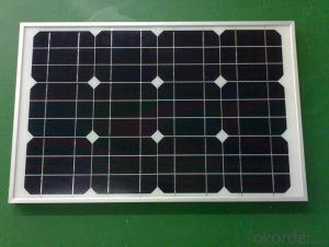
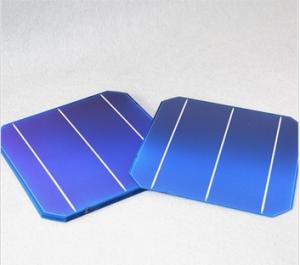
156x156 A Grade B Grade PV Silicon Solar Cell for Solar Panel
- Ref Price:
-

- Loading Port:
- China main port
- Payment Terms:
- TT OR LC
- Min Order Qty:
- 100 watt
- Supply Capability:
- 10000 watt/month
OKorder Service Pledge
OKorder Financial Service
You Might Also Like


156x156 A Grade B Grade PV Silicon Solar Cell for Solar Panel
Solar Module Summarize
Solar Module is the core part of solar PV power systems,also is the highest value part of it. The function of Solor Module is to convert the sun's radiation to electrical energy, or transfer it to battery and store in it, or to drive the load running.
The Product has been widely used in space and ground, it mainly used for power generation systems, charging systems, road lighting and traffic signs areas. It could offer a wide range of power and voltage, and with high conversion efficiency, and long service life.
Main Characteristic
our cells special features
1. High conversion efficiencies resulting in superior power output performance
2.Outstanding power output even in low light or high temperature conditions
3.Optimized design for ease of soldering and lamination
4.Long-term stability,reliability and performance
5.For 156P poly cells with high efficiency in photovoltaic conversion 16.3%-17.5%.
6.Low inverse current, high shunt resistance and high dependability.
7. Our poly cells efficiency include: 17%-18%.
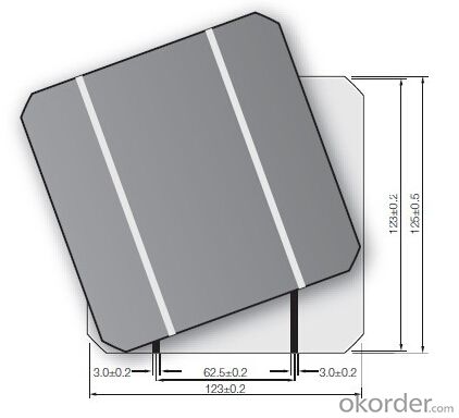
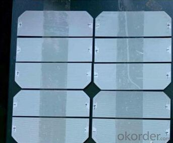
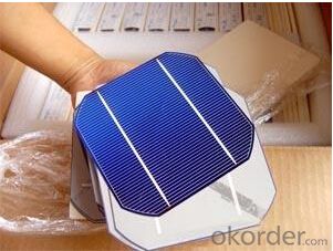
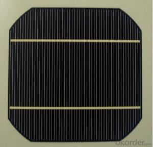
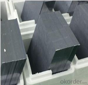
Product Pictures


- Q: Can solar silicon wafers be used in off-grid applications?
- Yes, solar silicon wafers can be used in off-grid applications. Solar panels made from silicon wafers are commonly used in off-grid applications as they can convert sunlight into electricity, providing a sustainable and renewable power source in remote locations without access to the grid.
- Q: What is the role of back contacts on solar silicon wafers?
- The role of back contacts on solar silicon wafers is to provide an electrical connection for the flow of current generated by the solar cells. They are typically made of metal and are placed on the backside of the wafer, opposite to the side exposed to sunlight. Back contacts help in collecting and conducting the electricity produced by the solar cells to the external circuit, enabling the utilization of solar energy for various applications.
- Q: What is the purpose of an encapsulant in a solar silicon wafer?
- The purpose of an encapsulant in a solar silicon wafer is to protect the wafer from moisture, dust, and other environmental factors, ensuring its long-term durability and performance. It also helps to enhance the efficiency of the solar cell by minimizing reflection and providing a smooth surface for better light absorption.
- Q: How do solar silicon wafers perform in coastal areas?
- Solar silicon wafers generally perform well in coastal areas as long as they are properly protected against the corrosive effects of saltwater and strong winds.
- Q: How do solar silicon wafers perform in high-wind conditions?
- Solar silicon wafers are generally designed to withstand high-wind conditions without significant damage. However, it is important to note that excessive wind speeds can potentially cause some stress or flexing on solar panels, including the silicon wafers. To ensure their performance and durability, solar panels are typically engineered with robust frames and mounting systems that can withstand strong winds. Additionally, regular maintenance and inspections are recommended to identify any potential issues and ensure the panels are properly secured.
- Q: What is the role of interconnection on solar silicon wafers?
- The role of interconnection on solar silicon wafers is to connect individual solar cells together in a series or parallel configuration to form a solar module. This interconnection allows for the flow of electricity generated by the solar cells, enabling the module to produce usable electricity.
- Q: Can solar silicon wafers be used in solar-powered electric fences?
- Yes, solar silicon wafers can be used in solar-powered electric fences. The wafers are used in solar panels to convert sunlight into electricity, which can then power the electric fence system.
- Q: What is the purity level of the silicon used in solar silicon wafers?
- The purity level of the silicon used in solar silicon wafers is typically around 99.9999%, also known as 6N purity.
- Q: What is the typical shelf life of a solar silicon wafer?
- The typical shelf life of a solar silicon wafer can vary depending on storage conditions, but it is generally expected to be around 1 to 2 years.
- Q: Can solar silicon wafers be used in space exploration missions?
- Yes, solar silicon wafers can be used in space exploration missions. They are commonly used in the construction of solar panels for spacecraft and satellites, allowing them to generate electrical power from sunlight in space.
Send your message to us
156x156 A Grade B Grade PV Silicon Solar Cell for Solar Panel
- Ref Price:
-
- Loading Port:
- China main port
- Payment Terms:
- TT OR LC
- Min Order Qty:
- 100 watt
- Supply Capability:
- 10000 watt/month
OKorder Service Pledge
OKorder Financial Service
Similar products


Hot products


Hot Searches
Related keywords

