


Monocrystalline Silicon Wafer, Solar Wafer, 156*156mm
- Ref Price:
-

- Loading Port:
- China Main Port
- Payment Terms:
- TT or LC
- Min Order Qty:
- 100 Pcs PCS
- Supply Capability:
- 700 MW/Per Year PCS/month
OKorder Service Pledge
OKorder Financial Service
You Might Also Like


Specification of Mono Silicon Wafer
We can provide you solar wafer 156*156mm Mono Wafers for your raw materials choice.
| Product name | Mono Wafer |
| Conductive type | P type |
| Square size wafer(mm) | 156×156±0.5 |
| Resistivity | 1~3 ohm |
| Corner(mm) | 150±0.5;165±0.5 |
| 195±0.5;200±0.5 | |
| Thickness (μm) | 200±20 |
| Total thickness(um) | ≤ 30 |
| Resistivity range(Ωcm) | 1-3 |
| Doping elements | Boron |
| Orientation | (100)±1° |
| Carbon content(atoms/cc) | ≤1.0E+17 |
| Oxygen content(atoms/cc) | ≤1.0E+18 |
| Lifetime(μs) | ≥10 |
| Surface quality | No crack, gap, missing Angle, perforated, silicon fell and stress |
| Warping degrees(warp/μm) | ≤50 |
| Neighbouring vertical degree | 90±0.5° |
| Side damage(mm) | ≤0.5mm(length)×0.3mm(width)(not more than 2 per wafer) |
| Line mark(μm) | ≤15 |
Usage and Applications of Mono Wafers
Mono Solar Wafer mainly used in Mono Solar Cells with reliable quality and trustful efficiency performance. Our Mono Wafers should be your best choice for raw materials.
Packaging & Delivery of Mono Wafers
Carton Box Package and Deliver by air. Mono Wafers should be avoid of sunshine, moist, and water.
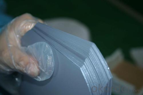
Factory Picture of Mono Wafers

Package Picture of Mono Wafers

- Q: What is the role of surface texturing on solar silicon wafers?
- The role of surface texturing on solar silicon wafers is to enhance light trapping and increase the absorption of sunlight. This texturing process creates rough surfaces on the wafer, which helps to scatter and trap light within the silicon material, allowing for better absorption and conversion of solar energy into electricity.
- Q: How is the bandgap of a solar silicon wafer determined?
- The bandgap of a solar silicon wafer is determined by measuring the energy difference between the valence band and the conduction band of the material. This can be done through various techniques, such as optical absorption spectroscopy or photoluminescence measurements. By analyzing the absorption or emission of light at different wavelengths, the bandgap energy can be accurately determined, providing crucial information for optimizing solar cell performance.
- Q: Can solar silicon wafers be used in disaster response vehicles?
- Yes, solar silicon wafers can be used in disaster response vehicles. They can be used to harness solar energy and power various systems and equipment in these vehicles, providing a sustainable and reliable source of power during emergency situations.
- Q: How are solar silicon wafers cleaned and maintained?
- Solar silicon wafers are cleaned and maintained through a multi-step process. First, any loose dirt or debris is removed by gently brushing or rinsing the surface. Next, a mild detergent or specialized cleaning solution is applied to remove stubborn dirt or oily residues. The wafers are then rinsed with deionized water to ensure no residue is left behind. Finally, the wafers are dried using clean, lint-free cloths or by air-drying. Regular inspections and maintenance, such as checking for any cracks or damages, are also essential to ensure optimal performance of the solar silicon wafers.
- Q: How are solar silicon wafers packaged and shipped?
- Solar silicon wafers are typically packaged and shipped in protective containers or trays. These containers are designed to securely hold the wafers in place and protect them from damage during transportation. The wafers are carefully stacked in the packaging with appropriate spacing to prevent any contact or scratching. Additionally, the packaging may include layers of foam or other cushioning materials to provide further protection. Once packaged, the wafers are typically shipped in bulk using suitable shipping methods, such as air freight or specialized carriers, to ensure safe delivery to their destination.
- Q: How are solar silicon wafers affected by temperature gradients?
- Solar silicon wafers are indeed affected by temperature gradients. When there is a temperature difference across the wafer, it can cause stress and strain within the material. This can lead to the development of cracks or even the complete failure of the wafer. To minimize these effects, manufacturers often use techniques like thermal annealing or doping with specific materials to enhance the wafer's thermal stability.
- Q: What is the role of metal contacts on solar silicon wafers?
- The role of metal contacts on solar silicon wafers is to provide electrical connections between the solar cells and external electrical circuitry. These contacts typically act as terminals for the flow of current, allowing the generated electricity to be collected and utilized.
- Q: The best process can be attached to explain!
- The silicon wafer contact material uses the quartz material, does not contact the metal material
- Q: How many watts can a piece of silicon produce
- A piece of silicon, has been able to integrate 160 thousand transistors. What a fine project! This is the crystallization of multidisciplinary collaborative efforts, is another milestone in the progress of science and technology.
- Q: What are the different sizes available for solar silicon wafers?
- Solar silicon wafers are available in various sizes, ranging from small to large dimensions. Common sizes include 125mm x 125mm, 156mm x 156mm, and 210mm x 210mm. However, the industry is constantly evolving, and larger wafer sizes such as 300mm x 300mm are being developed to improve solar panel efficiency and reduce costs.
1. Manufacturer Overview
| Location | |
| Year Established | |
| Annual Output Value | |
| Main Markets | |
| Company Certifications |
2. Manufacturer Certificates
| a) Certification Name | |
| Range | |
| Reference | |
| Validity Period |
3. Manufacturer Capability
| a) Trade Capacity | |
| Nearest Port | |
| Export Percentage | |
| No.of Employees in Trade Department | |
| Language Spoken: | |
| b) Factory Information | |
| Factory Size: | |
| No. of Production Lines | |
| Contract Manufacturing | |
| Product Price Range | |
Send your message to us
Monocrystalline Silicon Wafer, Solar Wafer, 156*156mm
- Ref Price:
-
- Loading Port:
- China Main Port
- Payment Terms:
- TT or LC
- Min Order Qty:
- 100 Pcs PCS
- Supply Capability:
- 700 MW/Per Year PCS/month
OKorder Service Pledge
OKorder Financial Service
Similar products


Hot products


Hot Searches

