


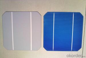
Silicon Solar Wafer - Mono Solar Cells 156mm*156mm in Bulk Quantity Low Price Stock 19.0
- Ref Price:
-

- Loading Port:
- Shanghai
- Payment Terms:
- TT OR LC
- Min Order Qty:
- 1000 pc
- Supply Capability:
- 100000 pc/month
OKorder Service Pledge
OKorder Financial Service
You Might Also Like


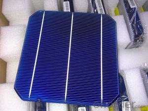
Brief Introduction
- Up to 20.0% efficiency, one of the highest performing mono crystalline cells on the market
- Three bus bars boosts current collection over the entire cell area, leading to higher fill factors
- Blue anti-reflecting coating allows more sunlight be captured and converted to electricity
- Finer, closer fingers improves charge collections for improved energy yield
- Lower light-induced degradation leads to greater power output over the entire module lifetime
- All solar cells are tightly classified to optimize output of module
- Maximum yield and longevity due to hotspot prevention
- Premium appearance results in a highly uniform and aesthetically appealing module
Specification
- Product Mono-crystalline silicon solar cell
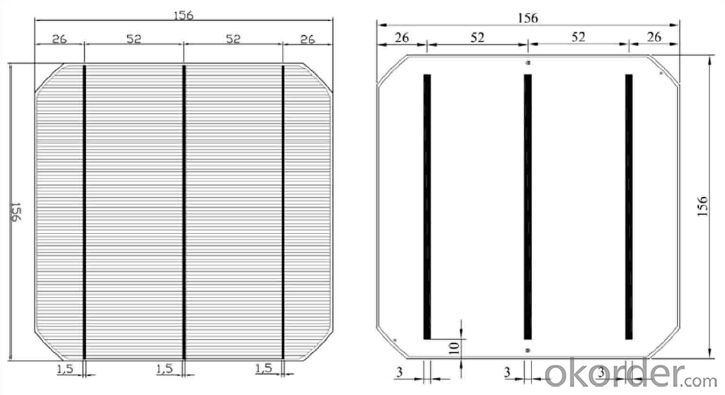
- Dimension 156 mm x 156 mm ± 0.5 mm
- Thickness 200 μm ± 30 μm
- Front 1.5 ± 0.1 mm busbar (silver)
- Silicon nitride antireflection coating
- Back 3.0 mm continuous soldering pads (silver)
- Back surface field (aluminum)
Electric performance parameters

- Testing conditions: 1000 W/m2, AM 1.5, 25 °C, Tolerance: Efficiency ± 0.2% abs., Pmpp ±1.5% rel.
- Imin : at 0.5 V
Light Intensity Dependence

Soldering Ability
- Peel Strength: > 1.0 N/mm (Pull soldered ribbon from busbar in 5 mm/s of 180°)
Dimension Figure

Quick Response
- Any time and anywhere, reply clients' email and solve all problems happen in the work at the first time.
- Remove clients doubts and offer the best solution at the first time.
- Give our clients the lastest news of the photovoltaic, update the newest stock informtion.
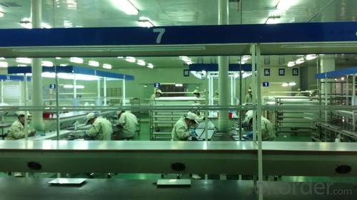
Production and Quality Control
- Precision cell efficiency sorting procedures
- Stringent criteria for color uniformity and appearance
- Reverse current and shunt resistance screening
- ISO9001,ISO14001 and OHSAS 18001,TUV Certificated


FAQ:
1. Q: Do you have your own factory?
A: Yes, we have. Our factory located in Jiangsu
2. Q: How can I visit your factory?
A: Before you visit,please contact us.We will show you the route or arrange a car to pick you up.
3. Q: Do you provide free sample?
A: Commenly we provide paid sample.
4. Q: Could you print our company LOGO on the nameplate and package?
A: Yes, we accept it.And need an Authorization Letter from you.
5. Q: Do you accept custom design on size?
A: Yes, if the size is reasonable.
6. Q: How can I be your agent in my country?
A: Please leave feedback. It's better for us to talk about details by email.
7. Q: Do you have solar project engineer who can guide me to install system?
A: Yes, we have a professional engineer team. They can teach you how to install a solar system.
- Q: What is the typical purity level of silicon used in solar silicon wafers?
- The typical purity level of silicon used in solar silicon wafers is around 99.9999%, also known as 6N purity.
- Q: What is the cutting fluid for solar wafer cutting?
- Solar wafer cuttingThe nine day of the moon is 1 | browse 4555Posted on 2011-03-08 14:06 best answerWire cutting equipment in Sweden, Japan, and domestic equipment;Sweden's MB and HCT devices are a little better;B, HCT, NTC and Ernst & Young wire cutting machine in the silicon wafer cutting silicon wafer cutting fluid and mortar requirementsLabel: cutting machine wire cutting machine silicon solar energyIn recent years, Chinese solar wafer cutting industry booming in Japan in 2008, another solar wafer multi wire cutting machine brand - Ernst & young, also started in the domestic debut, and big cost savings card, that technology has many advantages, more advanced. However, from the point of view of the effect of the use of domestic users, and NTC and MB and HCT in Switzerland, Ernst & Young in China there is a clear case of acclimatized.
- Q: How do solar silicon wafers contribute to energy independence?
- Solar silicon wafers contribute to energy independence by serving as the key component in solar panels, which convert sunlight into electricity. By harnessing the power of the sun, solar silicon wafers enable the generation of clean and renewable energy. This reduces our reliance on fossil fuels and foreign energy sources, promoting energy independence and a more sustainable future.
- Q: Are there any advancements in solar silicon wafer recycling technologies?
- Yes, there have been significant advancements in solar silicon wafer recycling technologies. With the increasing demand for renewable energy, researchers and companies have been working on developing more efficient and cost-effective methods to recycle silicon wafers used in solar panels. These advancements include improved separation and purification techniques, innovative recycling processes, and the development of new technologies to extract valuable materials from used solar panels. These advancements not only help reduce the environmental impact of solar panel production but also contribute to the circular economy by recovering valuable resources for reuse.
- Q: What are the different wafer orientations used in solar silicon wafer production?
- The different wafer orientations used in solar silicon wafer production are mainly three: (1) the most commonly used orientation is the <100> orientation, where the crystal structure is aligned along the <100> crystallographic direction; (2) the <111> orientation, which has a different crystal structure alignment; and (3) the <110> orientation, which is less commonly used but still finds some applications in certain solar cell designs.
- Q: Is the thickness of solar cell silicon wafer certain? Specifically how much
- 140-230 bar, see the specific requirements, most of the requirements of 200
- Q: Are there any initiatives to reduce the cost of solar silicon wafers?
- Yes, there are several initiatives aimed at reducing the cost of solar silicon wafers. These initiatives focus on improving the efficiency of production processes, implementing advanced manufacturing techniques, and exploring alternative materials for wafers. Additionally, research and development efforts are being made to enhance the efficiency of silicon wafers, which can ultimately contribute to cost reduction.
- Q: How do solar silicon wafers perform in snowy conditions?
- Solar silicon wafers generally perform well in snowy conditions, although their efficiency may be reduced. Snow can accumulate on the surface of the panels, blocking sunlight and affecting their ability to generate electricity. However, solar panels are designed to be self-cleaning to a certain extent, and as the snow melts or slides off, sunlight can reach the wafers again, allowing them to resume normal operation. Additionally, the dark color of the wafers helps absorb sunlight and aid in snow melt.
- Q: What is the purpose of a solar silicon wafer in solar cell production?
- The purpose of a solar silicon wafer in solar cell production is to serve as the base material on which the solar cells are built. The silicon wafer acts as a substrate onto which the various layers and components of the solar cell are deposited, allowing for the absorption and conversion of sunlight into electricity.
- Q: What is the role of light trapping in solar silicon wafers?
- The role of light trapping in solar silicon wafers is to enhance the absorption of sunlight by increasing the path length of light within the wafer. This allows for a greater amount of light to be absorbed, resulting in improved efficiency of the solar cell.
Send your message to us
Silicon Solar Wafer - Mono Solar Cells 156mm*156mm in Bulk Quantity Low Price Stock 19.0
- Ref Price:
-
- Loading Port:
- Shanghai
- Payment Terms:
- TT OR LC
- Min Order Qty:
- 1000 pc
- Supply Capability:
- 100000 pc/month
OKorder Service Pledge
OKorder Financial Service
Similar products


Hot products


Hot Searches
Related keywords

