

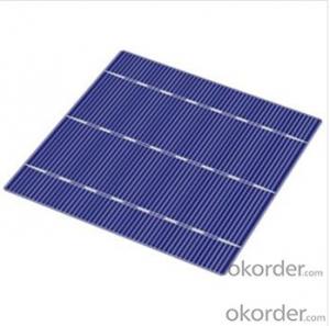
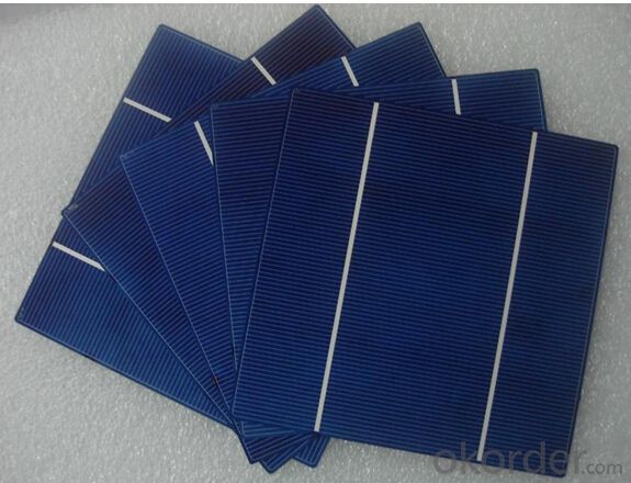
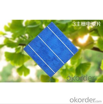

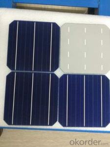
Silicon Wafer Solar Cell Panels - Monosolicion Poly 156mm*156mm
- Ref Price:
-

- Loading Port:
- China main port
- Payment Terms:
- TT OR LC
- Min Order Qty:
- 100 watt
- Supply Capability:
- 10000 watt/month
OKorder Service Pledge
Quality Product, Order Online Tracking, Timely Delivery
OKorder Financial Service
Credit Rating, Credit Services, Credit Purchasing
You Might Also Like


Monosolicion Solar Cells Poly 156mm*156mm
Typical electrical characteristics
Efficiency code | 1720 | 1740 | 1760 | 1780 | 1820 | 1840 | |
Efficiency (min) | (%) | 17.2 | 17.4 | 17.6 | 17.8 | 18.2 | 18.4 |
Pmax | (W) | 4.186 | 4.234 | 4.283 | 4.332 | 4.429 | 4.478 |
Voc | (V) | 0.631 | 0.632 | 0.634 | 0.636 | 0.640 | 0.642 |
Isc | (A) | 8.446 | 8.485 | 8.523 | 8.573 | 8.660 | 8.700 |
Vmp | (V) | 0.525 | 0.527 | 0.529 | 0.531 | 0.535 | 0.537 |
Imp | (A) | 7.973 | 8.035 | 8.097 | 8.160 | 8.280 | 8.340 |
Data under standard testing conditions(STC): 1,000W/m2, AM1.5, 25℃, Pmax: Positive power tolerance.
Typical teperature coefficients
Voltage | -2.08 | mV/K |
Current | +4.58 | mA/K |
Power | -0.40 | %/K |
Cell Picture


- Q: Can solar silicon wafers be used in concentrated solar power systems?
- Yes, solar silicon wafers can be used in concentrated solar power (CSP) systems. In CSP, mirrors or lenses concentrate sunlight onto a receiver, which can be a solar silicon wafer. The concentrated sunlight heats the wafer, generating electricity through the photovoltaic effect. So, solar silicon wafers are a viable option for harnessing solar energy in CSP systems.
- Q: Can solar silicon wafers be used in remote off-grid locations?
- Yes, solar silicon wafers can be used in remote off-grid locations. Solar panels made of silicon wafers are a reliable and efficient source of renewable energy, making them suitable for powering off-grid locations that lack access to traditional electricity grids. These panels can harness sunlight and convert it into electricity, providing a sustainable energy solution even in remote areas.
- Q: What is the typical reflectivity of a solar silicon wafer?
- The typical reflectivity of a solar silicon wafer is around 30% to 40%.
- Q: Are there any ongoing research efforts to enhance the efficiency of solar silicon wafers?
- Yes, there are ongoing research efforts to enhance the efficiency of solar silicon wafers. Various techniques and technologies, such as surface texturing, passivation layers, and advanced cell architectures, are being explored to improve light absorption, reduce recombination losses, and increase overall conversion efficiency. Additionally, scientists are investigating new materials like perovskites and tandem solar cells to further enhance the performance of silicon wafers. Continuous research and development in this field aim to make solar energy more cost-effective and viable for widespread adoption.
- Q: How do solar silicon wafers perform in areas with high air pollution?
- Solar silicon wafers may experience a decrease in performance in areas with high air pollution. The presence of pollutants like dust, smog, and particulate matter can accumulate on the surface of the solar panels, leading to reduced sunlight absorption and overall efficiency. The deposition of pollutants can block and scatter sunlight, diminishing the amount of energy that can be converted into electricity. Regular cleaning and maintenance of the panels are crucial to ensure optimal performance in such polluted areas.
- Q: What is the role of surface passivation layers on solar silicon wafers?
- The role of surface passivation layers on solar silicon wafers is to minimize the recombination of charge carriers, such as electrons and holes, at the surface of the wafer. These layers help improve the efficiency and performance of solar cells by reducing surface recombination losses, increasing the lifetime of charge carriers, and enhancing the overall electrical properties of the device.
- Q: What is the thickness of the semiconductor wafer used today?I have consulted some for solar wafers, heard now that the wafer thickness in 200~400 micron, but we need the wafer thickness requirements for high now, that for semiconductor wafer thickness is slightly higher than the solar energy, but I do not know how much is there in about 1 mm
- For integrated circuits: generally 4 inch wafer thickness of 0.520mm, the thickness of the 6 inch wafer
- Q: How does the efficiency of a solar silicon wafer vary with different light conditions?
- The efficiency of a solar silicon wafer varies with different light conditions. In optimal sunlight conditions, the efficiency is generally higher as the wafer can absorb a greater amount of sunlight and convert it into electricity more effectively. However, in low light conditions such as cloudy or overcast weather, the efficiency decreases as the wafer receives less sunlight to convert into electricity. Similarly, the efficiency may also be affected by the angle of incidence and shading caused by surrounding objects, which can decrease the overall efficiency of the wafer.
- Q: Are solar silicon wafers recyclable?
- Yes, solar silicon wafers are recyclable. The recycling process involves extracting valuable materials like silicon, silver, and aluminum from the wafers, which can then be reused in the production of new solar panels or other electronic devices.
- Q: From raw materials to finished products processing and production of the main links? Construction technology? Key issues of safety in production? What security measures are generally taken?
- (4): end shoulder growth after a long thin neck, to reduce the temperature and casting speed, the crystal diameter gradually increased to the desired size. (5) the diameter growth: after a long neck and shoulder end, by continuously adjusting casting speed and temperature, the crystal diameter maintained at between 2mm positive and negative, the diameter of fixed part is called the diameter part. Monocrystalline silicon wafer from the equal diameter part. (6) tail growth: if the rod is separated from the liquid surface, the effect force will cause the dislocation and slip line of the crystal rod. So in order to avoid the occurrence of this problem, the diameter of the crystal rod must be gradually reduced until it is a sharp point and separated from the liquid surface. This process is called tail growth. After a long period of time, the crystal rod is taken out of the furnace chamber for cooling for a period of time to complete a growth cycle.
Send your message to us
Silicon Wafer Solar Cell Panels - Monosolicion Poly 156mm*156mm
- Ref Price:
-
- Loading Port:
- China main port
- Payment Terms:
- TT OR LC
- Min Order Qty:
- 100 watt
- Supply Capability:
- 10000 watt/month
OKorder Service Pledge
Quality Product, Order Online Tracking, Timely Delivery
OKorder Financial Service
Credit Rating, Credit Services, Credit Purchasing
Similar products


Hot products


Hot Searches
Related keywords

