

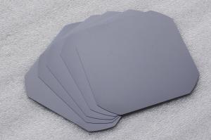


Solar Silicon Wafer - Monocrystalline Grade
- Ref Price:
-

- Loading Port:
- Shanghai Port
- Payment Terms:
- TT or LC
- Min Order Qty:
- 100Pieces PCS
- Supply Capability:
- 700 MW/Per Year PCS/month
OKorder Service Pledge
OKorder Financial Service
You Might Also Like


Specification of Mono Silicon Wafers
We can provide you solar wafer both156*156 and 125*125mm, Mono and Poly
Solar Wafers for your raw materials choice.
| Product name | Mono Wafer |
| Conductive type | P type |
| Square size wafer(mm) | 156×156±0.5 |
| Resistivity range | 1~3 ohm |
| Corner(mm) | 150±0.5;165±0.5 |
| 195±0.5;200±0.5 | |
| Thickness (μm) | 200±20 |
| Total thickness(um) | ≤ 30 |
| Resistivity range(Ωcm) | 1-3 |
| Doping elements | Boron |
| Orientation | (100)±1° |
| Carbon content(atoms/cc) | ≤1.0E+17 |
| Oxygen content(atoms/cc) | ≤1.0E+18 |
| Lifetime(μs) | ≥10 |
| Surface quality | No crack, gap, missing Angle, perforated, silicon fell and stress |
| Warping degrees(warp/μm) | ≤50 |
| Neighbouring vertical degree | 90±0.5° |
| Side damage(mm) | ≤0.5mm(length)×0.3mm(width)(not more than 2 per wafer) |
| Line mark(μm) | ≤15 |
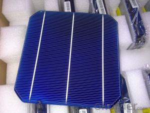
Usage and Applications of Mono Solar Wafers
Mono Solar Wafers mainly used in Solar Cells with reliable quality and trustful efficiency performance. Our Wafers should be your best choice for raw materials.
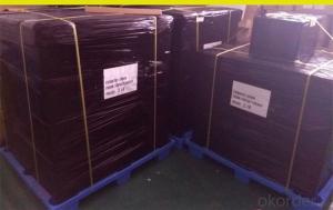
Packaging & Delivery of Mono Solar Wafers
Carton Box Package and Deliver by air. It should be avoid of moist, water and shaking to protect the safety of Solar Cells.
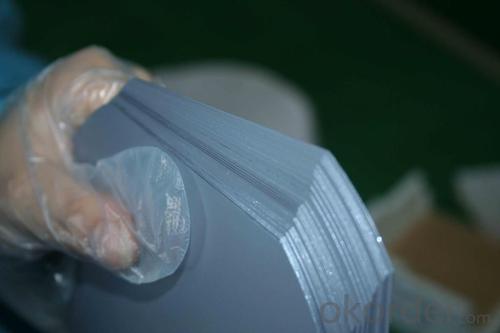
Factory Picture of Mono Solar Wafers

Package Picture of Mono Solar Wafers

- Q: Are there any initiatives to reduce the environmental impact of solar silicon wafer production?
- Yes, there are several initiatives underway to reduce the environmental impact of solar silicon wafer production. These initiatives focus on implementing cleaner and more sustainable manufacturing processes, improving energy efficiency, reducing water usage, and minimizing waste generation during production. Additionally, research and development efforts are ongoing to explore alternative materials and technologies that can further enhance the environmental performance of solar silicon wafer production.
- Q: Can solar silicon wafers be used in solar-powered water desalination?
- Yes, solar silicon wafers can be used in solar-powered water desalination. These wafers are commonly used in photovoltaic (PV) panels to convert sunlight into electricity. By utilizing solar silicon wafers, solar-powered desalination systems can harness solar energy to power the desalination process, making it a sustainable and environmentally friendly solution for producing fresh water from seawater.
- Q: How are solar silicon wafers protected from vandalism?
- Solar silicon wafers are typically protected from vandalism by installing them in secure locations, such as rooftops or fenced-off areas, that are difficult for unauthorized individuals to access. Additionally, some solar installations may employ security cameras, alarms, or other monitoring systems to deter and detect any potential acts of vandalism.
- Q: Are there any limitations to using solar silicon wafers in solar cells?
- Yes, there are limitations to using solar silicon wafers in solar cells. Some of these limitations include the high cost of production and the environmental impact associated with the extraction and purification of silicon. Additionally, silicon wafers are relatively brittle and can be prone to cracking or breaking under certain conditions. Furthermore, the efficiency of silicon solar cells can be reduced by factors such as temperature, shading, and a limited absorption spectrum. However, ongoing research and development efforts are focused on addressing these limitations and improving the performance and cost-effectiveness of silicon-based solar cells.
- Q: Can solar silicon wafers be damaged by hail or other weather conditions?
- Yes, solar silicon wafers can be damaged by hail or other severe weather conditions. Hailstones can cause physical impact damage, leading to cracks or fractures on the wafers. Additionally, extreme weather conditions like heavy storms, high winds, or lightning strikes can also pose risks to the integrity of solar panels, including the silicon wafers. It is essential to consider the potential impact of weather conditions and take appropriate measures to protect solar panels from potential damage.
- Q: How do solar silicon wafers perform in snowy conditions?
- Solar silicon wafers generally perform well in snowy conditions, although their efficiency may be slightly affected. While snow can reduce the amount of sunlight reaching the solar panels, the white surface of the snow can also reflect sunlight back onto the panels, increasing their performance. Additionally, solar panels are typically installed at an angle, allowing snow to slide off more easily. In regions with heavy snowfall, it is recommended to install solar panels at a steeper angle or use snow management techniques to ensure optimal performance.
- Q: Are there any alternative materials to silicon for solar wafer production?
- Yes, there are several alternative materials to silicon for solar wafer production. Some examples include thin-film solar cells made from materials like cadmium telluride (CdTe), copper indium gallium selenide (CIGS), and perovskites. These materials offer advantages such as flexibility, lower manufacturing costs, and higher efficiency potential. However, they also have their own challenges in terms of stability, scalability, and toxicity. Ongoing research and development efforts are focused on improving the performance and commercial viability of these alternative materials for wider adoption in solar energy production.
- Q: What is the impact of impurities on the efficiency of solar silicon wafers?
- Impurities in solar silicon wafers can significantly affect their efficiency. These impurities can alter the electrical properties of the material, leading to reduced conversion of sunlight into electricity. For instance, impurities like boron or phosphorus can introduce additional charge carriers, increasing the recombination rate and decreasing the overall efficiency. Moreover, impurities can also create energy barriers within the material, hindering the movement of charge carriers and limiting the wafers' performance. Therefore, it is crucial to ensure high purity levels in silicon wafers to maximize their efficiency in converting solar energy.
- Q: Hello, the last time you gave me the answer on the silicon chip let me learn a lot, I would like to ask here, sapphire crystal density you know?
- Mineral name: corundum.Hard brittle materialChemical composition: Al 2 O 3; can contain Fe, Ti, Cr, V, Mn and other elements.Crystalline state.Crystal system: three party system;
- Q: What is the purpose of a backsheet in a solar silicon wafer?
- The purpose of a backsheet in a solar silicon wafer is to protect the solar cells from external elements such as moisture, dust, and physical damage. It acts as a barrier and provides insulation to the backside of the solar module, ensuring the longevity and efficiency of the solar panel.
1. Manufacturer Overview
| Location | |
| Year Established | |
| Annual Output Value | |
| Main Markets | |
| Company Certifications |
2. Manufacturer Certificates
| a) Certification Name | |
| Range | |
| Reference | |
| Validity Period |
3. Manufacturer Capability
| a) Trade Capacity | |
| Nearest Port | |
| Export Percentage | |
| No.of Employees in Trade Department | |
| Language Spoken: | |
| b) Factory Information | |
| Factory Size: | |
| No. of Production Lines | |
| Contract Manufacturing | |
| Product Price Range | |
Send your message to us
Solar Silicon Wafer - Monocrystalline Grade
- Ref Price:
-
- Loading Port:
- Shanghai Port
- Payment Terms:
- TT or LC
- Min Order Qty:
- 100Pieces PCS
- Supply Capability:
- 700 MW/Per Year PCS/month
OKorder Service Pledge
OKorder Financial Service
Similar products


Hot products


Hot Searches
Related keywords

