


Silicon Wafer Solar Cell - High Quality A Grade Mono Crystalline 5V 18.8%
- Ref Price:
-

- Loading Port:
- Shanghai
- Payment Terms:
- TT OR LC
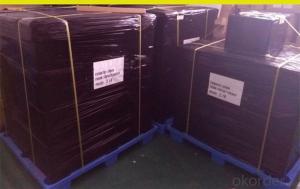
- Min Order Qty:
- 1000 pc
- Supply Capability:
- 100000 pc/month
OKorder Service Pledge
OKorder Financial Service
You Might Also Like


Specifications
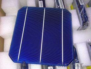
hot sale solar cell
1.16.8%~18.25% high efficiency
2.100% checked quality
3.ISO9001/ISO14001/TUV/CE/UL
4.stable performance
We can offer you the best quality products and services, don't miss !
POLY6'(156*156)
Polycrystalline Silicon Solar cell
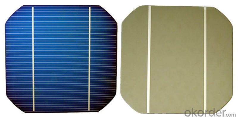
Physical Characteristics
Dimension: 156mm×156mm±0.5mm
Diagonal: 220mm±0.5mm
Thickness(Si): 200±20 μm
Front(-) Back(+)
Blue anti-reflecting coating (silicon nitride); Aluminum back surface field;
1.5mm wide bus bars; 2.0mm wide soldering pads;
Distance between bus bars: 51mm . Distance between bus bars :51mm .
Electrical Characteristics
Efficiency(%) | 18.00 | 17.80 | 17.60 | 17.40 | 17.20 | 16.80 | 16.60 | 16.40 | 16.20 | 16.00 | 15.80 | 15.60 |
Pmpp(W) | 4.33 | 4.29 | 4.24 | 4.19 | 4.14 | 4.09 | 4.04 | 3.99 | 3.94 | 3.90 | 3.86 | 3.82 |
Umpp(V) | 0.530 | 0.527 | 0.524 | 0.521 | 0.518 | 0.516 | 0.514 | 0.511 | 0.509 | 0.506 | 0.503 | 0.501 |
Impp(A) | 8.159 | 8.126 | 8.081 | 8.035 | 7.990 | 7.938 | 7.876 | 7.813 | 7.754 | 7.698 | 7.642 | 7.586 |
Uoc(V) | 0.633 | 0.631 | 0.628 | 0.625 | 0.623 | 0.620 | 0.618 | 0.617 | 0.615 | 0.613 | 0.611 | 0.609 |
Isc(A) | 8.709 | 8.677 | 8.629 | 8.578 | 8.531 | 8.478 | 8.419 | 8.356 | 8.289 | 8.220 | 8.151 | 8.083 |

MONO5'(125*125mm)165
Monocrystalline silicon solar cell
Physical Characteristics
Dimension: 125mm×125mm±0.5mm
Diagonal: 165mm±0.5mm
Thickness(Si): 200±20 μm
Front(-) Back(+)
Blue anti-reflecting coating(silicon nitride); Aluminum back surface field;
1.6mmwide bus bars; 2.5mm wide soldering pads;
Distance between bus bars: 61mm . Distance between bus bars :61mm .
Electrical Characteristics
Efficiency(%) | 19.40 | 19.20 | 19.00 | 18.80 | 18.60 | 18.40 | 18.20 | 18.00 | 17.80 | 17.60 | 17.40 | 17.20 |
Pmpp(W) | 2.97 | 2.94 | 2.91 | 2.88 | 2.85 | 2.82 | 2.79 | 2.76 | 2.73 | 2.70 | 2.67 | 2.62 |
Umpp(V) | 0.537 | 0.535 | 0.533 | 0.531 | 0.527 | 0.524 | 0.521 | 0.518 | 0.516 | 0.515 | 0.513 | 0.509 |
Impp(A) | 5.531 | 5.495 | 5.460 | 5.424 | 5.408 | 5.382 | 5.355 | 5.328 | 5.291 | 5.243 | 5.195 | 4.147 |
Uoc(V) | 0.637 | 0.637 | 0.636 | 0.635 | 0.633 | 0.630 | 0.629 | 0.629 | 0.628 | 0.626 | 0.626 | 0.625 |
Isc(A) | 5.888 | 5.876 | 5.862 | 5.848 | 5.839 | 5.826 | 5.809 | 5.791 | 5.779 | 5.756 | 5.293 | 5.144 |

FAQ:
Q:How can i get some sample?
A:Yes , if you want order ,sample is not a problem.
Q:How about your solar panel efficency?
A: Our product efficency around 17.25%~18.25%.
Q:What’s the certificate you have got?
A: we have overall product certificate of ISO9001/ISO14001/CE/TUV/UL
- Q: How are solar silicon wafers interconnected to form solar modules?
- Solar silicon wafers are interconnected to form solar modules through a process called stringing and tabbing. This involves soldering thin metal strips called busbars onto the front and back surfaces of the wafers, creating electrical connections. The busbars serve as positive and negative terminals, allowing the flow of electricity between the cells. Multiple interconnected cells are then encapsulated in a protective layer, such as glass or polymer, to form a complete solar module.
- Q: What are the main considerations when selecting a solar silicon wafer supplier?
- When selecting a solar silicon wafer supplier, the main considerations include the quality and reliability of the wafers, the supplier's track record and reputation in the industry, their manufacturing capabilities and capacity, their ability to meet specific requirements or customizations, and the overall cost-effectiveness of their products. Additionally, factors such as the supplier's commitment to sustainability and environmental responsibility, their technical support and customer service, and their adherence to industry standards and certifications should also be taken into account.
- Q: How are solar silicon wafers affected by humidity and moisture?
- Solar silicon wafers are negatively affected by humidity and moisture. Exposure to high humidity or moisture can cause corrosion and oxidation on the surface of the wafers, which can impair their performance and efficiency. Moisture can also lead to the formation of water droplets or films on the surface, creating a barrier that reduces the amount of sunlight absorbed by the wafers. Additionally, humidity can increase the risk of electrical leakage and insulation failure in the solar cells. Therefore, it is crucial to protect solar silicon wafers from excessive humidity and moisture to maintain their optimal functioning.
- Q: What is the role of passivation on solar silicon wafers?
- The role of passivation on solar silicon wafers is to minimize surface recombination and increase the efficiency of the solar cell. Passivation helps to reduce defects and traps on the surface of the wafer, allowing for better charge carrier separation and collection, which ultimately leads to improved performance of the solar cell.
- Q: What is the role of a solar silicon wafer in solar energy generation?
- The role of a solar silicon wafer in solar energy generation is to serve as the main component of a solar cell. These wafers are made from highly purified silicon and are responsible for converting sunlight into electricity through the photovoltaic effect. The wafer acts as a platform for other layers and materials to be added, such as metal contacts and anti-reflective coatings, to enhance the efficiency of the solar cell. Ultimately, the solar silicon wafer plays a crucial role in capturing and converting solar energy into usable electricity.
- Q: What is the impact of light-induced degradation on solar silicon wafers?
- Light-induced degradation, also known as LID, has a significant impact on solar silicon wafers. It causes a decrease in the efficiency and performance of the solar cells over time. LID occurs when the silicon material is exposed to light, particularly in the presence of boron or oxygen impurities. This exposure leads to the creation of defects and traps within the material, which results in a decrease in the solar cell's ability to generate electricity. Consequently, LID reduces the overall power output of the solar panel and requires additional measures to mitigate its effects, such as anti-LID coatings or improved cell designs.
- Q: Process flow of wafer wafer ultrasonic cleaning machine?
- Plasma cleaning method, which is characterized in that the process parameters of gas flushing process is: the chamber pressure of 15 mTorr, process gas flow 300sccm, time 3S; process parameters of starting process is: the chamber pressure of 15 mTorr, process gas flow on the electrode 300sccm, power 300W, time Ss
- Q: How does the efficiency of a solar silicon wafer change with snow cover?
- The efficiency of a solar silicon wafer decreases with snow cover. Snow acts as an insulator, preventing sunlight from reaching the wafer and reducing its ability to generate electricity. Additionally, snow can also cause shading on the surface of the wafer, further reducing its efficiency.
- Q: What is the role of back surface field in solar silicon wafers?
- The role of the back surface field in solar silicon wafers is to enhance the efficiency of the solar cell by reducing recombination and increasing the collection of charge carriers generated by sunlight. It creates a strong electric field at the back surface of the wafer, pushing the minority carriers towards the front surface, where they can be collected and harnessed to generate electricity.
- Q: How are solar silicon wafers protected from handling errors during installation?
- Solar silicon wafers are protected from handling errors during installation through careful procedures and the use of protective measures. These include using specialized handling tools and equipment to ensure minimal contact with the wafers, implementing cleanroom environments to prevent contamination, and using protective packaging materials to safeguard the wafers during transportation and installation. Additionally, proper training and adherence to strict protocols by the installation personnel further minimize the risk of handling errors and potential damage to the solar silicon wafers.
Send your message to us
Silicon Wafer Solar Cell - High Quality A Grade Mono Crystalline 5V 18.8%
- Ref Price:
-
- Loading Port:
- Shanghai
- Payment Terms:
- TT OR LC
- Min Order Qty:
- 1000 pc
- Supply Capability:
- 100000 pc/month
OKorder Service Pledge
OKorder Financial Service
Similar products


Hot products


Hot Searches
Related keywords

