


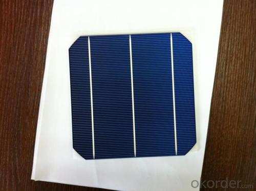


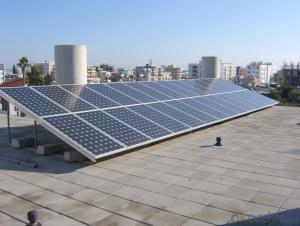
Silicon Wafer Solar Cell - High Quality A Grade Mono Crystalline 5V 17.2%
- Ref Price:
-

- Loading Port:
- Shanghai
- Payment Terms:
- TT OR LC
- Min Order Qty:
- 1000 pc
- Supply Capability:
- 100000 pc/month
OKorder Service Pledge
OKorder Financial Service
You Might Also Like


Specifications
hot sale solar cell
1.16.8%~18.25% high efficiency
2.100% checked quality
3.ISO9001/ISO14001/TUV/CE/UL
4.stable performance
We can offer you the best quality products and services, don't miss !
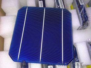
POLY6'(156*156)
Polycrystalline Silicon Solar cell
Physical Characteristics
Dimension: 156mm×156mm±0.5mm
Diagonal: 220mm±0.5mm
Thickness(Si): 200±20 μm
Front(-) Back(+)
Blue anti-reflecting coating (silicon nitride); Aluminum back surface field;
1.5mm wide bus bars; 2.0mm wide soldering pads;
Distance between bus bars: 51mm . Distance between bus bars :51mm .
Electrical Characteristics
Efficiency(%) | 18.00 | 17.80 | 17.60 | 17.40 | 17.20 | 16.80 | 16.60 | 16.40 | 16.20 | 16.00 | 15.80 | 15.60 |
Pmpp(W) | 4.33 | 4.29 | 4.24 | 4.19 | 4.14 | 4.09 | 4.04 | 3.99 | 3.94 | 3.90 | 3.86 | 3.82 |
Umpp(V) | 0.530 | 0.527 | 0.524 | 0.521 | 0.518 | 0.516 | 0.514 | 0.511 | 0.509 | 0.506 | 0.503 | 0.501 |
Impp(A) | 8.159 | 8.126 | 8.081 | 8.035 | 7.990 | 7.938 | 7.876 | 7.813 | 7.754 | 7.698 | 7.642 | 7.586 |
Uoc(V) | 0.633 | 0.631 | 0.628 | 0.625 | 0.623 | 0.620 | 0.618 | 0.617 | 0.615 | 0.613 | 0.611 | 0.609 |
Isc(A) | 8.709 | 8.677 | 8.629 | 8.578 | 8.531 | 8.478 | 8.419 | 8.356 | 8.289 | 8.220 | 8.151 | 8.083 |

MONO5'(125*125mm)165
Monocrystalline silicon solar cell
Physical Characteristics
Dimension: 125mm×125mm±0.5mm
Diagonal: 165mm±0.5mm
Thickness(Si): 200±20 μm
Front(-) Back(+)
Blue anti-reflecting coating(silicon nitride); Aluminum back surface field;
1.6mmwide bus bars; 2.5mm wide soldering pads;
Distance between bus bars: 61mm . Distance between bus bars :61mm .
Electrical Characteristics
Efficiency(%) | 19.40 | 19.20 | 19.00 | 18.80 | 18.60 | 18.40 | 18.20 | 18.00 | 17.80 | 17.60 | 17.40 | 17.20 |
Pmpp(W) | 2.97 | 2.94 | 2.91 | 2.88 | 2.85 | 2.82 | 2.79 | 2.76 | 2.73 | 2.70 | 2.67 | 2.62 |
Umpp(V) | 0.537 | 0.535 | 0.533 | 0.531 | 0.527 | 0.524 | 0.521 | 0.518 | 0.516 | 0.515 | 0.513 | 0.509 |
Impp(A) | 5.531 | 5.495 | 5.460 | 5.424 | 5.408 | 5.382 | 5.355 | 5.328 | 5.291 | 5.243 | 5.195 | 4.147 |
Uoc(V) | 0.637 | 0.637 | 0.636 | 0.635 | 0.633 | 0.630 | 0.629 | 0.629 | 0.628 | 0.626 | 0.626 | 0.625 |
Isc(A) | 5.888 | 5.876 | 5.862 | 5.848 | 5.839 | 5.826 | 5.809 | 5.791 | 5.779 | 5.756 | 5.293 | 5.144 |

FAQ:
Q:How can i get some sample?
A:Yes , if you want order ,sample is not a problem.
Q:How about your solar panel efficency?
A: Our product efficency around 17.25%~18.25%.
Q:What’s the certificate you have got?
A: we have overall product certificate of ISO9001/ISO14001/CE/TUV/UL
- Q: How are solar silicon wafers cleaned during the manufacturing process?
- Solar silicon wafers are cleaned during the manufacturing process through a combination of mechanical, chemical, and thermal methods. Initially, the wafers are rinsed with deionized water to remove any loose particles or impurities. Then, a chemical solution is applied to dissolve and remove organic and inorganic contaminants. This is followed by a rinse with deionized water again to eliminate any remaining chemicals. Lastly, the wafers may undergo a thermal treatment to ensure complete cleanliness.
- Q: Are solar silicon wafers affected by temperature changes?
- Yes, solar silicon wafers are affected by temperature changes. Temperature fluctuations can impact the efficiency and performance of solar silicon wafers, as higher temperatures can lead to a decrease in their power output. On the other hand, extreme cold temperatures can also affect their performance, although to a lesser extent. Therefore, it is important to consider temperature management and cooling techniques to optimize the performance of solar silicon wafers.
- Q: What are the impurities in a solar silicon wafer?
- The impurities commonly found in a solar silicon wafer include boron, phosphorus, and trace amounts of other elements such as aluminum, iron, and copper.
- Q: What's the connection between silicon wafer and wafer
- Why is the semiconductor wafer has to be large because he wants to cut into small square chips
- Q: Can solar silicon wafers be used in thin-film solar cell technology?
- No, solar silicon wafers cannot be used in thin-film solar cell technology. Thin-film solar cells use different materials, such as amorphous silicon, cadmium telluride, or copper indium gallium selenide, to capture sunlight and convert it into electricity.
- Q: What is the impact of impurities on the durability of solar silicon wafers?
- Impurities in solar silicon wafers can have a significant impact on their durability. These impurities can affect the structural integrity and electrical properties of the wafers, leading to reduced efficiency and shorter lifespan of the solar cells. Impurities like metal ions or oxygen can introduce defects in the crystal lattice, causing degradation and increased recombination of charge carriers. This can result in reduced power output and decreased overall performance of the solar panels. Therefore, minimizing impurities and ensuring high purity silicon is crucial for enhancing the durability and longevity of solar silicon wafers.
- Q: How are solar silicon wafers protected from fire hazards?
- Solar silicon wafers are protected from fire hazards through the implementation of safety measures such as fire-resistant encapsulation materials, fire suppression systems, and proper installation techniques. These measures help prevent the ignition and spread of fires, ensuring the safety and reliability of solar panels.
- Q: Can solar silicon wafers be used in mobile or portable solar chargers?
- Yes, solar silicon wafers can be used in mobile or portable solar chargers. These chargers utilize photovoltaic cells made from silicon wafers to convert sunlight into electricity, allowing for the charging of various mobile devices on the go.
- Q: Are there any alternatives to solar silicon wafers?
- Yes, there are several alternatives to solar silicon wafers. Some of the alternatives include thin-film solar cells made from materials like cadmium telluride (CdTe), copper indium gallium selenide (CIGS), and organic photovoltaic (OPV) cells. These alternatives have different advantages and disadvantages compared to silicon wafers, such as lower production costs, flexibility, and better performance in low-light conditions. However, silicon wafers still dominate the solar market due to their high efficiency and proven reliability.
- Q: How do solar silicon wafers convert sunlight into electricity?
- Solar silicon wafers convert sunlight into electricity through a process called the photovoltaic effect. When sunlight hits the surface of the silicon wafer, it excites the electrons in the silicon atoms, causing them to break free from their atoms and create an electric current. This current is then captured and harnessed to generate usable electricity.
Send your message to us
Silicon Wafer Solar Cell - High Quality A Grade Mono Crystalline 5V 17.2%
- Ref Price:
-
- Loading Port:
- Shanghai
- Payment Terms:
- TT OR LC
- Min Order Qty:
- 1000 pc
- Supply Capability:
- 100000 pc/month
OKorder Service Pledge
OKorder Financial Service
Similar products


Hot products


Hot Searches
Related keywords

