


Monocrystalline Silicon Wafer,125*125, Solar Wafers
- Ref Price:
-

- Loading Port:
- Shanghai Port
- Payment Terms:
- TT or LC
- Min Order Qty:
- 100 Pieces PCS
- Supply Capability:
- 700MW/Per Year PCS/month
OKorder Service Pledge
OKorder Financial Service
You Might Also Like


Specifications of Mono Solar Wafer
Monocrystalline solar wafer 125*125mm
Conductivity Type: P type
Dopant: Boron
Resistivity: 1~3 ohm
thickness: 200um.
| Product name | Mono Wafer |
| Conductive type | P type |
| Square size wafer(mm) | 125×125±0.5 mm |
| Resistivity | 1~3 ohm |
| Corner(mm) | 150±0.5;165±0.5 |
| 195±0.5;200±0.5 | |
| Thickness (μm) | 200±20 |
| Total thickness(um) | ≤ 30 |
| Resistivity range(Ωcm) | 1-3 |
| Doping elements | Boron |
| Orientation | (100)±1° |
| Carbon content(atoms/cc) | ≤1.0E+17 |
| Oxygen content(atoms/cc) | ≤1.0E+18 |
| Lifetime(μs) | ≥10 |
| Surface quality | No crack, gap, missing Angle, perforated, silicon fell and stress |
| Warping degrees(warp/μm) | ≤50 |
| Neighbouring vertical degree | 90±0.5° |
| Side damage(mm) | ≤0.5mm(length)×0.3mm(width)(not more than 2 per wafer) |
| Line mark(μm) | ≤15 |
Advantages of Mono Solar Wafers
1. High efficiency and High power.2. Long-term electrical stability.
3. Lowest price and Fastest delivery.
4. Good quality and good service.
5. Bulk supply
6. Good Warranty
7. Big Sale
8. More than 25 years on the lifetime.
Usage and Applications of Mono Solar Wafers
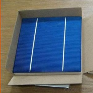
Mono Solar wafers is used to make Solar Cells. With high quality and stable quality. Our Solar Wafers can greatly improve the performance of Solar Cells.
Packaging & Delivery of Mono Solar Wafers
Carton Box Package and Deliver by air.It should be noticed that it should be avoid of water, sunshine and moist.
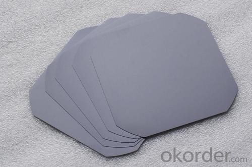
Wafer Factory Picture of Mono Solar Wafers

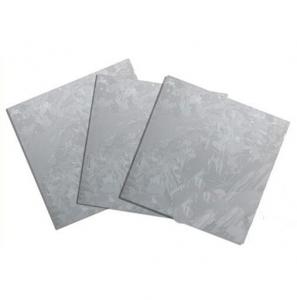
Package Picture of Mono Solar Wafers

- Q: How are solar silicon wafers connected in a solar panel?
- Solar silicon wafers are typically connected in a solar panel through a process known as cell interconnection. This involves soldering or bonding the individual wafers together using conductive materials such as silver or copper. The wafers are then connected in series or parallel to form strings or modules, respectively, creating a network of interconnected cells that generate electricity when exposed to sunlight.
- Q: What are the current trends in solar silicon wafer technology?
- Some of the current trends in solar silicon wafer technology include the development of thinner wafers to reduce material costs and improve efficiency, the use of high-efficiency monocrystalline wafers for higher power output, the adoption of diamond wire sawing techniques for more precise and cost-effective wafer production, and the exploration of new materials and processes like multi-junction cells and bifacial modules for enhanced energy generation.
- Q: What are the potential future advancements in solar silicon wafer technology?
- Some potential future advancements in solar silicon wafer technology include the development of thinner and more efficient wafers, advancements in multi-junction solar cells, improvements in manufacturing processes, and the integration of silicon wafer technology with other materials such as perovskites or tandem cells. Additionally, research is being conducted to enhance the stability and durability of silicon wafers, increase their flexibility for use in various applications, and explore new methods for reducing production costs. Overall, the future of solar silicon wafer technology holds promise for higher efficiency, improved performance, and wider adoption of solar energy.
- Q: What is the difference between silicon wafer P111 and P100
- If the crystal is body centered cubic lattice, the crystal orientation through the cube on the diagonal atoms
- Q: Can solar silicon wafers be used in solar-powered waste management systems?
- Yes, solar silicon wafers can be used in solar-powered waste management systems. These wafers are essential components in solar panels, which can generate electricity from sunlight. By harnessing solar energy, waste management systems can operate efficiently and sustainably, powering various processes such as waste collection, recycling, and treatment.
- Q: What are the different types of solar silicon wafers available?
- The different types of solar silicon wafers available include monocrystalline, polycrystalline, and thin-film. Monocrystalline wafers are made from a single crystal structure, making them highly efficient but more expensive. Polycrystalline wafers are made from multiple crystal structures and are slightly less efficient but more affordable. Thin-film wafers are made by depositing a thin layer of silicon on a substrate and offer flexibility and lower production costs, but they have lower efficiency compared to crystalline wafers.
- Q: What is the role of solar silicon wafers in disaster response and recovery?
- Solar silicon wafers play a crucial role in disaster response and recovery by providing a reliable source of clean energy. These wafers are used to manufacture solar panels, which can be quickly deployed in disaster-stricken areas to generate electricity. This renewable energy source helps power emergency response efforts, including communication systems, lighting, medical equipment, and water purification systems. Solar silicon wafers enable more sustainable and resilient disaster response, reducing dependence on traditional power sources and ensuring a continuous supply of electricity in times of crisis.
- Q: What is the expected payback period for a solar panel with silicon wafers?
- The expected payback period for a solar panel with silicon wafers can vary depending on various factors such as the initial cost of the panel, its efficiency, the amount of sunlight it receives, and the local electricity rates. On average, solar panels with silicon wafers have a payback period ranging from 5 to 10 years, but this can be shorter in areas with high solar irradiation and favorable incentives or longer in areas with lower solar resource and limited incentives.
- Q: What is the typical doping material used in solar silicon wafers?
- The typical doping material used in solar silicon wafers is usually phosphorous or boron.
- Q: Can solar silicon wafers be used in agricultural crop drying systems?
- Yes, solar silicon wafers can be used in agricultural crop drying systems.
1. Manufacturer Overview
| Location | |
| Year Established | |
| Annual Output Value | |
| Main Markets | |
| Company Certifications |
2. Manufacturer Certificates
| a) Certification Name | |
| Range | |
| Reference | |
| Validity Period |
3. Manufacturer Capability
| a) Trade Capacity | |
| Nearest Port | |
| Export Percentage | |
| No.of Employees in Trade Department | |
| Language Spoken: | |
| b) Factory Information | |
| Factory Size: | |
| No. of Production Lines | |
| Contract Manufacturing | |
| Product Price Range | |
Send your message to us
Monocrystalline Silicon Wafer,125*125, Solar Wafers
- Ref Price:
-
- Loading Port:
- Shanghai Port
- Payment Terms:
- TT or LC
- Min Order Qty:
- 100 Pieces PCS
- Supply Capability:
- 700MW/Per Year PCS/month
OKorder Service Pledge
OKorder Financial Service
Similar products


Hot products


Hot Searches
Related keywords

