

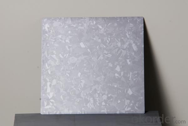


Solar Cell Silicon Wafer - Polycrystalline Solar Silicon Wafer, 125*125mm
- Ref Price:
-

- Loading Port:
- Shanghai Port
- Payment Terms:
- TT or LC
- Min Order Qty:
- 100 Pieces PCS
- Supply Capability:
- 700MW/Per Year PCS/month
OKorder Service Pledge
OKorder Financial Service
You Might Also Like


Specifications of Poly Solar Wafers
|
Product name |
Poly Wafer |
| Conductive type | P Type |
| Square size wafer (mm) | 125×125±0.5 |
| 219.20±0.5 | |
| Corner (mm)
|
1±0.5、45°±10º |
| 200±20 | |
| Total thickness(um) | ≤40 |
| Resistivity ranges(Ωcm) | 1-3 |
| Doping elements | boron |
| Carbon content(atoms/cc) | ≤8*1017 |
| Oxygen content(atoms/cc) | ≤1*1018 |
| Lifetime(μs) | ≥2 |
| Surface quality | No crack, gap, missing Angle, perforated, window, microcrystalline |
| Warping degrees(μm) | ≤50 |
| Neighbouring vertical degree | 90±0.5° |
| Side damage(mm) | ≤0.5mm(length)×0.3mm(width),(not more than 2 per wafer) |
| Line mark(μm) | ≤15 |
Advantages of Poly Solar Wafers
1. High efficiency and High power.
2. Long-term electrical stability.
3. Lowest price and Fastest delivery.
4. Good quality and good service.
5. Bulk supply
6. Good Warranty
7. Big Sale
8. More than 25 years on the lifetime.
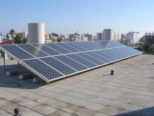
Usage and Applications of Poly Solar Wafer
Poly Solar Wafers mainly used to make Poly Solar Cells. Our wafers are your best choice of raw material, which can greatly improve the performance of the Solar Cells and Solar Modules.
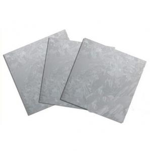
Packaging & Delivery of Poly Solar Wafer
Carton Box Package and Deliver by air. It should be noticed that it should be avoid of water, sunshine and moist.
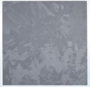
Factory of Solar Wafers

Package Picture of Solar Wafer

- Q: What are the advantages of using silicon for solar wafers?
- There are several advantages of using silicon for solar wafers. Firstly, silicon is abundantly available as it is the second most abundant element on Earth, making it a cost-effective choice for solar panel production. Secondly, silicon has excellent electrical properties, allowing for efficient conversion of sunlight into electricity. Additionally, silicon is a stable and durable material, ensuring the longevity of solar panels. Lastly, silicon-based solar panels have a high efficiency rate, meaning they can generate more electricity from the same amount of sunlight compared to other materials.
- Q: How are solar silicon wafers inspected for surface defects?
- Solar silicon wafers are inspected for surface defects through various methods such as visual inspection, automated optical inspection (AOI), and scanning electron microscopy (SEM). Visual inspection involves visually examining the wafers under proper lighting conditions to identify any visible defects or anomalies. AOI uses specialized cameras and computer algorithms to detect and analyze surface defects, ensuring a high level of accuracy and efficiency. SEM, on the other hand, offers a more detailed and magnified view of the wafer surface, enabling the identification of even minute defects at a microscopic level. These inspection methods play a crucial role in ensuring the quality and efficiency of solar silicon wafers.
- Q: Are solar silicon wafers affected by UV radiation?
- Yes, solar silicon wafers are affected by UV radiation. UV radiation can cause degradation and damage to the silicon material over time, reducing the efficiency and lifespan of solar panels. To mitigate this, solar panels often incorporate protective coatings or materials that can minimize the impact of UV radiation.
- Q: What is the typical thickness tolerance for a solar silicon wafer?
- The typical thickness tolerance for a solar silicon wafer is around ±10 micrometers.
- Q: What is the impact of impurities on the reliability of solar silicon wafers?
- Impurities in solar silicon wafers can have a significant impact on their reliability. These impurities, such as metal contaminants or oxygen atoms, can affect the electrical properties and overall performance of the wafers. They can introduce defects and decrease the efficiency of solar cells, leading to reduced power output and shorter lifespan. Therefore, ensuring high purity levels in solar silicon wafers is crucial for maintaining their reliability and optimizing solar panel performance.
- Q: Are there any advancements in solar silicon wafer surface texturing techniques?
- Yes, there have been significant advancements in solar silicon wafer surface texturing techniques. Researchers and industry experts have been continuously working on improving the efficiency and performance of solar cells, and one area of focus has been the texture of silicon wafers. Various texturing techniques like chemical etching, laser processing, and plasma techniques have been developed to enhance light trapping and reduce reflection, ultimately increasing the overall efficiency of solar cells. These advancements in surface texturing techniques have played a crucial role in the development of more efficient and cost-effective solar panels.
- Q: What is the expected payback period for a solar panel with silicon wafers?
- The expected payback period for a solar panel with silicon wafers can vary depending on various factors such as the initial cost of the panel, its efficiency, the amount of sunlight it receives, and the local electricity rates. On average, solar panels with silicon wafers have a payback period ranging from 5 to 10 years, but this can be shorter in areas with high solar irradiation and favorable incentives or longer in areas with lower solar resource and limited incentives.
- Q: Why can silicon chips store information? Even if it is a miniature circuit, unplug the power on the use of electricity, there is no electricity in the silicon chip, in the form of what capacity storage
- Storage of information is not a silicon chip, called memory, which is a transistor electronic components, called the silicon chip is made of silicon crystals directly on the transistor array,
- Q: What are the main challenges in the production of solar silicon wafers?
- The main challenges in the production of solar silicon wafers include the high energy consumption and environmental impact associated with the manufacturing process. Additionally, maintaining consistent quality and purity of the silicon material, ensuring optimal utilization of raw materials, and minimizing production costs are also significant challenges. Furthermore, managing the delicate handling and processing of the wafers to prevent damage or contamination is crucial for achieving high-performance solar cells.
- Q: What are the different types of solar silicon wafers?
- There are primarily three types of solar silicon wafers: monocrystalline, polycrystalline, and thin-film. Monocrystalline wafers are made from a single crystal structure, offering high efficiency but are more expensive. Polycrystalline wafers are made from multiple crystals, providing lower efficiency but at a lower cost. Thin-film wafers are made from a thin layer of semiconductor material deposited onto a substrate, offering flexibility and lower costs, but with lower efficiency compared to crystalline silicon wafers.
1. Manufacturer Overview
| Location | |
| Year Established | |
| Annual Output Value | |
| Main Markets | |
| Company Certifications |
2. Manufacturer Certificates
| a) Certification Name | |
| Range | |
| Reference | |
| Validity Period |
3. Manufacturer Capability
| a) Trade Capacity | |
| Nearest Port | |
| Export Percentage | |
| No.of Employees in Trade Department | |
| Language Spoken: | |
| b) Factory Information | |
| Factory Size: | |
| No. of Production Lines | |
| Contract Manufacturing | |
| Product Price Range | |
Send your message to us
Solar Cell Silicon Wafer - Polycrystalline Solar Silicon Wafer, 125*125mm
- Ref Price:
-
- Loading Port:
- Shanghai Port
- Payment Terms:
- TT or LC
- Min Order Qty:
- 100 Pieces PCS
- Supply Capability:
- 700MW/Per Year PCS/month
OKorder Service Pledge
OKorder Financial Service
Similar products


Hot products


Hot Searches

