


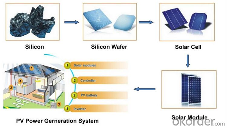
High Efficiency 6X6 Inch Silicon Wafer for Solar Cell
- Ref Price:
-

- Loading Port:
- Shanghai
- Payment Terms:
- TT OR LC
- Min Order Qty:
- 10000 pc
- Supply Capability:
- 200000 pc/month
OKorder Service Pledge
OKorder Financial Service
You Might Also Like


Quick Details | |||||
| Place of Origin: | China (Mainland) | Model Number: | 156P-2BB | ||
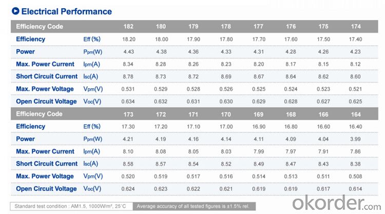
| Material:: | Polycrystalline Silicon | Size:: | 156mmx156mm or 6 inch | Max. Power:: | 4.2watts |
| efficiency:: | 16%-17.2% | busbar:: | 2 | Color: | Dark Blue |
| Voltage:: | 0.508V-0.53V | Thickness:: | 190um±20um | ||
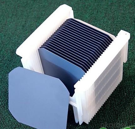
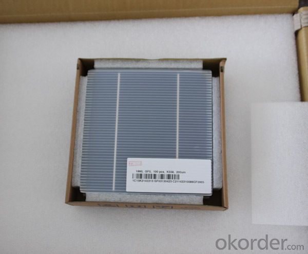
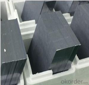
Packaging & Delivery
| Packaging Details: | 100pcs in one box,1000pcs per carton, standard export carton Silicon Wafer for Solar Cell |
| Delivery Detail: | 5-7 days after received the payment |
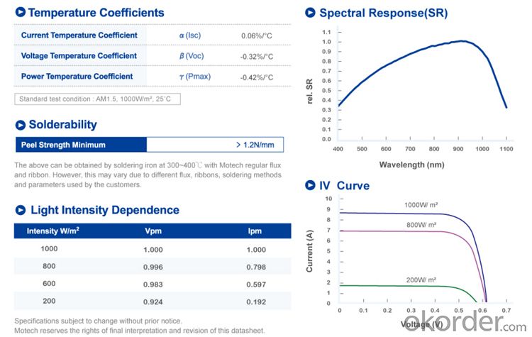
Specifications
Best Solar Cell Price
1.6*6 solar cell
2. 4.2W
3.2BB
Best Price Per Watt High Efficiency 6X6 Inch Silicon Wafer for Solar Cell
Product Description
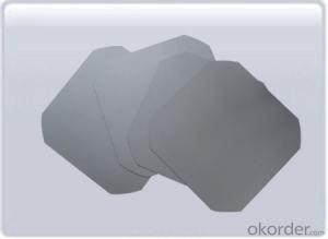
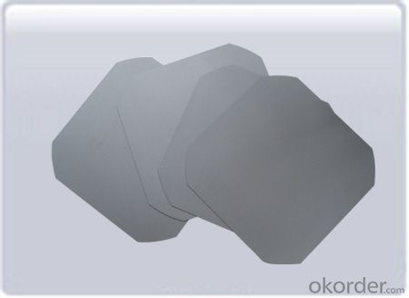
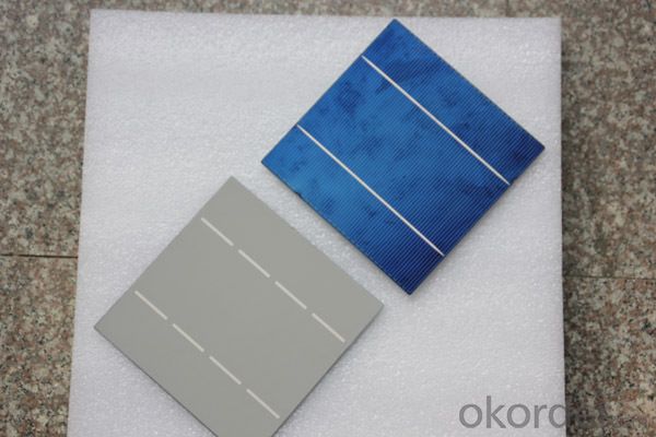
Silicon Wafer for Solar Cell
Dimension: 156x156mm
Front: Blue silicon nitride anti-reflection coating
2.0mm silver busbars
Back: Full-surface aluminum back-surface field
2.0mm( silver/ aluminum) discontinuous soldering pads
Image
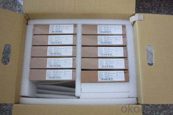
Packaging & Shipping
1. Item are only shipped after PAYMENT is received
2. Originally our solar cells are 100 pieces per box, 10 boxes per carton.
2. Please check out your ADDRESS carefully when processing order.
3. Please CONTACT us ASAP if you haven't received the parcel.
Shipping will be made via EMS, DHL, Fedex, UPS , TNT etc
- Q: What is the effect of temperature on the efficiency of a solar silicon wafer?
- The temperature has a significant effect on the efficiency of a solar silicon wafer. As the temperature increases, the efficiency of the wafer decreases. This is because higher temperatures can lead to increased resistance in the wafer, which in turn reduces the flow of electricity. Additionally, higher temperatures can cause the semiconductor properties of the wafer to degrade, resulting in a decrease in its ability to convert sunlight into electricity. Therefore, controlling and minimizing the temperature of the solar silicon wafer is crucial for maximizing its efficiency and overall performance.
- Q: How are solar silicon wafers cleaned and maintained?
- Solar silicon wafers are cleaned and maintained through a combination of mechanical and chemical processes. The cleaning process typically involves removing dust, dirt, and other contaminants that accumulate on the surface of the wafers. This is done using brushes, deionized water, and mild cleaning solutions. Additionally, regular maintenance includes monitoring the performance of the solar panels, inspecting for any damages or defects, and ensuring proper functioning of the electrical connections.
- Q: How are solar silicon wafers protected from electrical faults or short circuits?
- Solar silicon wafers are protected from electrical faults or short circuits through the implementation of various protective measures. One common method is the use of anti-reflective coatings on the surface of the wafers, which not only enhance their efficiency but also act as a protective layer. Additionally, they are typically encapsulated within a durable, non-conductive material, such as glass or a polymer, to provide insulation and safeguard against electrical faults. Furthermore, electrical connections and circuits within the solar panels are carefully designed and installed to minimize the risk of short circuits and ensure proper functioning of the system.
- Q: What is the purpose of surface texturing in solar silicon wafers?
- The purpose of surface texturing in solar silicon wafers is to increase the efficiency of solar cells by reducing reflection and maximizing light absorption.
- Q: Are there any limitations to using solar silicon wafers in solar cells?
- Yes, there are limitations to using solar silicon wafers in solar cells. Some of these limitations include the high cost of production and the environmental impact associated with the extraction and purification of silicon. Additionally, silicon wafers are relatively brittle and can be prone to cracking or breaking under certain conditions. Furthermore, the efficiency of silicon solar cells can be reduced by factors such as temperature, shading, and a limited absorption spectrum. However, ongoing research and development efforts are focused on addressing these limitations and improving the performance and cost-effectiveness of silicon-based solar cells.
- Q: How are solar silicon wafers protected from chemical damage during manufacturing?
- Solar silicon wafers are protected from chemical damage during manufacturing through various methods. One common technique involves using a thin layer of passivation material, such as silicon nitride or silicon dioxide, to create a protective coating on the surface of the wafer. This coating acts as a barrier, preventing direct contact between the wafer and potentially harmful chemicals. Additionally, proper handling and storage protocols are followed to minimize exposure to chemicals that could cause damage.
- Q: What is the impact of wafer resistivity on solar silicon wafer performance?
- The wafer resistivity of a solar silicon wafer has a significant impact on its performance. Lower resistivity wafers have higher conductivity, allowing for more efficient flow of electrical current. This leads to improved conversion of sunlight into electricity and higher overall solar cell efficiency. On the other hand, higher resistivity wafers may result in increased resistive losses, reducing the effectiveness of the solar cell. Therefore, selecting silicon wafers with appropriate resistivity is crucial in optimizing solar panel performance.
- Q: Can solar silicon wafers be made transparent for specific applications?
- Yes, solar silicon wafers can be made transparent for specific applications by implementing various techniques such as thinning the wafer thickness, reducing crystal defects, and applying anti-reflective coatings. These measures allow a certain amount of light to pass through the wafer while maintaining its functionality as a solar cell. This transparency can be beneficial for applications like building-integrated photovoltaics (BIPV) or solar windows, where aesthetics and light transmission are important factors.
- Q: What is the impact of stress and strain on solar silicon wafers?
- The impact of stress and strain on solar silicon wafers can be detrimental to their performance and reliability. Excessive stress and strain can cause cracking, warping, and even fracture in the wafers, leading to decreased electrical efficiency and potential failure of the solar cells. It is crucial to minimize stress and strain during manufacturing, handling, and installation processes to maintain the structural integrity and optimal functioning of the solar silicon wafers.
- Q: How is the voltage output of a solar silicon wafer regulated?
- The voltage output of a solar silicon wafer is regulated through the use of a device called a charge controller. The charge controller ensures that the voltage output from the solar panel remains within a safe range by regulating the flow of current from the panel to the battery or grid. It prevents overcharging of the battery and protects the electrical system from voltage spikes.
Send your message to us
High Efficiency 6X6 Inch Silicon Wafer for Solar Cell
- Ref Price:
-
- Loading Port:
- Shanghai
- Payment Terms:
- TT OR LC
- Min Order Qty:
- 10000 pc
- Supply Capability:
- 200000 pc/month
OKorder Service Pledge
OKorder Financial Service
Similar products


Hot products


Hot Searches
Related keywords

