


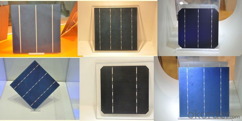

Solar Silicon Wafer for Sale - High Quality A Grade Polycrystalline 5V 16.8% Solar Cell
- Ref Price:
-

- Loading Port:
- Shanghai
- Payment Terms:
- TT OR LC
- Min Order Qty:
- 1000 pc
- Supply Capability:
- 100000 pc/month
OKorder Service Pledge
OKorder Financial Service
You Might Also Like


Specifications
hot sale solar cell
1.16.8%~18.25% high efficiency
2.100% checked quality
3.ISO9001/ISO14001/TUV/CE/UL
4.stable performance
We can offer you the best quality products and services, don't miss !
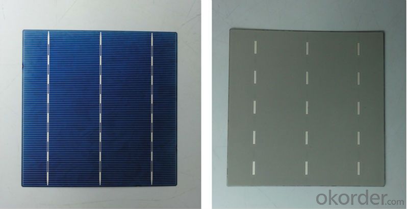
POLY6'(156*156)
Polycrystalline Silicon Solar cell
Physical Characteristics
Dimension: 156mm×156mm±0.5mm
Diagonal: 220mm±0.5mm
Thickness(Si): 200±20 μm
Front(-) Back(+)
Blue anti-reflecting coating (silicon nitride); Aluminum back surface field;
1.5mm wide bus bars; 2.0mm wide soldering pads;
Distance between bus bars: 51mm . Distance between bus bars :51mm .
Electrical Characteristics
Efficiency(%) | 18.00 | 17.80 | 17.60 | 17.40 | 17.20 | 16.80 | 16.60 | 16.40 | 16.20 | 16.00 | 15.80 | 15.60 |
Pmpp(W) | 4.33 | 4.29 | 4.24 | 4.19 | 4.14 | 4.09 | 4.04 | 3.99 | 3.94 | 3.90 | 3.86 | 3.82 |
Umpp(V) | 0.530 | 0.527 | 0.524 | 0.521 | 0.518 | 0.516 | 0.514 | 0.511 | 0.509 | 0.506 | 0.503 | 0.501 |
Impp(A) | 8.159 | 8.126 | 8.081 | 8.035 | 7.990 | 7.938 | 7.876 | 7.813 | 7.754 | 7.698 | 7.642 | 7.586 |
Uoc(V) | 0.633 | 0.631 | 0.628 | 0.625 | 0.623 | 0.620 | 0.618 | 0.617 | 0.615 | 0.613 | 0.611 | 0.609 |
Isc(A) | 8.709 | 8.677 | 8.629 | 8.578 | 8.531 | 8.478 | 8.419 | 8.356 | 8.289 | 8.220 | 8.151 | 8.083 |

MONO5'(125*125mm)165
Monocrystalline silicon solar cell
Physical Characteristics
Dimension: 125mm×125mm±0.5mm
Diagonal: 165mm±0.5mm
Thickness(Si): 200±20 μm
Front(-) Back(+)
Blue anti-reflecting coating(silicon nitride); Aluminum back surface field;
1.6mmwide bus bars; 2.5mm wide soldering pads;
Distance between bus bars: 61mm . Distance between bus bars :61mm .
Electrical Characteristics
Efficiency(%) | 19.40 | 19.20 | 19.00 | 18.80 | 18.60 | 18.40 | 18.20 | 18.00 | 17.80 | 17.60 | 17.40 | 17.20 |
Pmpp(W) | 2.97 | 2.94 | 2.91 | 2.88 | 2.85 | 2.82 | 2.79 | 2.76 | 2.73 | 2.70 | 2.67 | 2.62 |
Umpp(V) | 0.537 | 0.535 | 0.533 | 0.531 | 0.527 | 0.524 | 0.521 | 0.518 | 0.516 | 0.515 | 0.513 | 0.509 |
Impp(A) | 5.531 | 5.495 | 5.460 | 5.424 | 5.408 | 5.382 | 5.355 | 5.328 | 5.291 | 5.243 | 5.195 | 4.147 |
Uoc(V) | 0.637 | 0.637 | 0.636 | 0.635 | 0.633 | 0.630 | 0.629 | 0.629 | 0.628 | 0.626 | 0.626 | 0.625 |
Isc(A) | 5.888 | 5.876 | 5.862 | 5.848 | 5.839 | 5.826 | 5.809 | 5.791 | 5.779 | 5.756 | 5.293 | 5.144 |

FAQ:
Q:How can i get some sample?
A:Yes , if you want order ,sample is not a problem.
Q:How about your solar panel efficency?
A: Our product efficency around 17.25%~18.25%.
Q:What’s the certificate you have got?
A: we have overall product certificate of ISO9001/ISO14001/CE/TUV/UL
- Q: How do solar silicon wafers perform in hot climates?
- Solar silicon wafers perform well in hot climates as they are designed to withstand high temperatures. However, excessive heat can slightly decrease their efficiency, leading to a small reduction in energy output. Nonetheless, solar panels are typically engineered with cooling mechanisms to counteract the effects of heat, ensuring optimal performance even in hot climates.
- Q: What are the different types of junction box sealants used on solar silicon wafers?
- There are primarily two types of junction box sealants used on solar silicon wafers - silicone-based sealants and hot melt adhesives. Silicone-based sealants offer excellent resistance to moisture, UV radiation, and temperature variations, making them ideal for outdoor solar applications. Hot melt adhesives, on the other hand, provide strong bonding properties and are relatively easier to apply during the manufacturing process. Ultimately, the choice of sealant depends on the specific requirements and conditions of the solar panel installation.
- Q: How is a junction box connector integrated into a solar silicon wafer?
- A junction box connector is typically integrated into a solar silicon wafer through a soldering or welding process. The connector is attached to the wafer's conductive contacts, allowing for the secure connection of electrical wires. This integration ensures the efficient transfer of electricity generated by the solar panel.
- Q: How do solar silicon wafers affect the overall flexibility of a solar panel?
- Solar silicon wafers have a minimal impact on the overall flexibility of a solar panel. While the wafers themselves are rigid and inflexible, they are typically mounted onto a flexible substrate, such as metal or plastic, which allows the solar panel to maintain some degree of flexibility. The main factor affecting the flexibility of a solar panel is the choice of substrate material rather than the silicon wafers.
- Q: Why integrated circuits are rectangular and the silicon chips are round
- The disk that you see is a wafer. This disk is not only the production of a chip, but N multiple chips are produced in this disk.
- Q: What is the role of a mounting structure in a solar silicon wafer?
- The role of a mounting structure in a solar silicon wafer is to provide support and stability to the wafer, allowing it to be securely attached to a solar panel or other mounting surface. The mounting structure ensures that the wafer is properly positioned and protected, maximizing its exposure to sunlight and optimizing its energy generation capabilities.
- Q: How does the efficiency of a solar silicon wafer change with panel orientation?
- The efficiency of a solar silicon wafer can vary with panel orientation. Generally, when solar panels are oriented towards the sun's path, they receive maximum sunlight and, therefore, tend to be more efficient. However, deviations from the optimal orientation can lead to a reduction in efficiency. Factors such as the angle of incidence, shading, and the specific location's latitude also influence the efficiency of the solar silicon wafer with respect to panel orientation.
- Q: Can solar silicon wafers be used in solar-powered cell towers?
- Yes, solar silicon wafers can be used in solar-powered cell towers. These wafers serve as the foundation for solar panels that generate electricity from sunlight, which can then be used to power cell towers.
- Q: How do solar silicon wafers perform in different weather conditions?
- Solar silicon wafers perform well in a variety of weather conditions. While they may produce slightly less electricity during cloudy or overcast weather, they still generate energy due to their ability to convert sunlight into electricity. Rain, snow, or extreme temperatures do not significantly affect their performance, as they are designed to withstand such conditions. However, it is important to note that they perform optimally under direct sunlight, resulting in the highest energy production.
- Q: What are the different types of solar silicon wafers?
- There are mainly three types of solar silicon wafers: monocrystalline, polycrystalline, and amorphous. Monocrystalline wafers are made from a single crystal structure and are known for their high efficiency. Polycrystalline wafers are made from multiple crystals and are less expensive but slightly less efficient. Amorphous wafers are non-crystalline and have the lowest efficiency, but they are flexible and can be used in flexible solar panels.
Send your message to us
Solar Silicon Wafer for Sale - High Quality A Grade Polycrystalline 5V 16.8% Solar Cell
- Ref Price:
-
- Loading Port:
- Shanghai
- Payment Terms:
- TT OR LC
- Min Order Qty:
- 1000 pc
- Supply Capability:
- 100000 pc/month
OKorder Service Pledge
OKorder Financial Service
Similar products


Hot products


Hot Searches
Related keywords

