
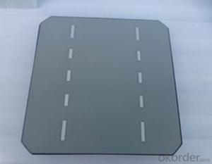
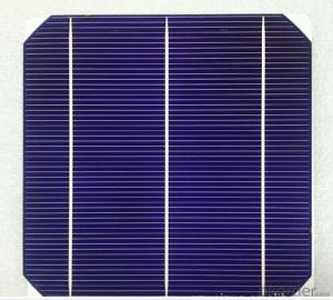
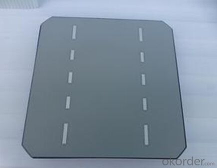
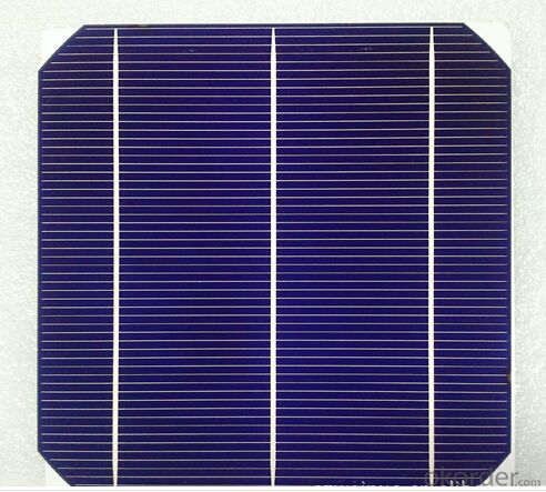
Industrial Silicon Wafer Solar Cells / 156mm Mono Solar Cell
- Ref Price:
-

- Loading Port:
- China main port
- Payment Terms:
- TT OR LC
- Min Order Qty:
- 100 watt
- Supply Capability:
- 10000 watt/month
OKorder Service Pledge
OKorder Financial Service
You Might Also Like


Monocrystalline Silicon Solar Cell/156mm Mono Solar Cell
Type:156M
Appearance:156×1565㎜±0.5mm;diagonal:R=100mm
Main fence wide:1.4-1.5mm back electrode wide:2-2.5mm
Fence line qty:90
Cell thickness:220um±20um
Eff(%) | 18.00- 18.10 | 18.10- 18.20 | 18.20- 18.30 | 18.30- 18.40 | 18.40- 18.50 | 18.50- 18.60 | 18.60- 18.70 | 18.70- 18.80 | 18.80- 18.90 | 18.9- 19.0 | 19.1- 19.1 | 19.1- 19.2 |
Pm(W) | 4.30 | 4.33 | 4.35 | 4.37 | 4.40 | 4.42 | 4.44 | 4.47 | 4.49 | 4.52 | 4.54 | 4.56 |
Isc(A) | 8.71 | 8.73 | 8.76 | 8.77 | 8.78 | 8.82 | 8.83 | 8.85 | 8.86 | 8.88 | 8.9 | 8.93 |
Im(A) | 8.19 | 8.21 | 8.24 | 8.26 | 8.30 | 8.33 | 8.35 | 8.39 | 8.42 | 8.45 | 8.47 | 8.51 |
Voc(V) | 0.630 | 0.631 | 0.632 | 0.633 | 0.634 | 0.634 | 0.635 | 0.636 | 0.637 | 0.637 | 0.638 | 0.64 |
Vm(V) | 0.527 | 0.528 | 0.529 | 0.531 | 0.531 | 0.532 | 0.534 | 0.534 | 0.535 | 0.536 | 0.537 | 0.538 |
FF(%) | 78.6 | 78.7 | 78.8 | 79.0 | 79.2 | 79.3 | 79.5 | 79.6 | 79.8 | 80 | 80 | 80 |
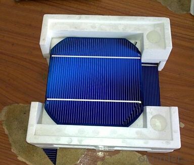
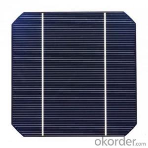
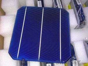
Picture show


Shipping
1. Shipment shall be made only after PAYMENT is received.
2. Please do inform us your DETAILED ADDRESS AND CONTACT INFOMATION before shipment.
3. Shipment shall be made in THREE WORKING DAYS.
2. Shipment shall be via EMS, DHL, Fedex,UPS etc.
- Q: Are there any regulations or standards for solar silicon wafers?
- Yes, there are regulations and standards for solar silicon wafers. These regulations and standards are put in place to ensure the quality, efficiency, and safety of solar silicon wafers used in the production of solar cells and panels. They cover various aspects such as the purity of the silicon, thickness and uniformity of the wafer, electrical properties, and environmental sustainability. These regulations and standards are developed and enforced by organizations such as the International Electrotechnical Commission (IEC) and the American Society for Testing and Materials (ASTM). Compliance with these regulations and standards is important for the reliable and effective operation of solar energy systems.
- Q: Can solar silicon wafers be used in harsh climates?
- Yes, solar silicon wafers can be used in harsh climates. They are designed to withstand extreme weather conditions, including high temperatures, humidity, and even freezing temperatures. Additionally, they are often made with protective coatings to ensure durability and longevity in harsh environments.
- Q: What is the purpose of an encapsulant in a solar silicon wafer?
- The purpose of an encapsulant in a solar silicon wafer is to protect the wafer from external factors such as moisture, dirt, and mechanical stress, ensuring its durability and longevity. It also helps in maintaining the electrical properties of the wafer and enhances its overall performance by reducing reflection and increasing light absorption.
- Q: Can solar silicon wafers be used in solar-powered water pumps?
- Yes, solar silicon wafers can be used in solar-powered water pumps. The wafers are used to convert sunlight into electricity, which can then be used to power the water pump.
- Q: How do solar silicon wafers contribute to sustainable development goals?
- Solar silicon wafers contribute to sustainable development goals by enabling the production of clean and renewable energy. They are the key component in solar panels, which harness sunlight and convert it into electricity without emitting greenhouse gases or other harmful pollutants. By promoting the use of solar energy, silicon wafers help reduce reliance on fossil fuels, mitigate climate change, and support the transition towards a more sustainable and environmentally friendly energy system. Additionally, the manufacturing of solar silicon wafers can create jobs and stimulate economic growth, contributing to the goal of sustainable economic development.
- Q: What are the current trends in solar silicon wafer technology?
- Some of the current trends in solar silicon wafer technology include the shift towards thinner wafers, such as the adoption of 180-200 micrometer thickness, which reduces material costs and improves efficiency. Another trend is the development of larger wafer sizes, with the industry moving from 156 mm to 182 mm and even 210 mm sizes, enabling higher power output and reducing installation costs. Additionally, there is a focus on improving the overall quality and uniformity of wafers to optimize solar cell performance.
- Q: How does the efficiency of a solar silicon wafer change with snow cover?
- The efficiency of a solar silicon wafer decreases with snow cover. Snow acts as an insulating layer, preventing sunlight from reaching the wafer and reducing its ability to convert solar energy into electricity. Additionally, snow can cause shading and blockage of sunlight, further decreasing the efficiency of the solar panel.
- Q: What specific steps should be used to clean the wafer? A little more detail
- But when these two semiconductors are connected, they form a "P-N junction". When the current through the wire to the chip, the electron will be pushed to the P area, in the P area of the electron and hole compound, and then will be in the form of photon energy, which is the principle of LED luminescence. The wavelength of light is the color of light, which is determined by the material that forms the P-N junction. The utility model is a display screen which is used for displaying various information such as text, graphics, image, animation, quotation, video, video signal, etc. by controlling the display mode of the semiconductor light emitting diode.
- Q: I grew up in the silicon chip Ag particles, the size of about a few hundred nanometers, I would like to ask how I do before the TEM sample?
- And then use the copper net fishing, so that particles attached to the copper network.
- Q: How is the demand for solar silicon wafers expected to grow in the future?
- The demand for solar silicon wafers is expected to grow significantly in the future due to the increasing adoption of solar energy as a sustainable and renewable source of power. As countries and industries shift towards clean energy solutions, the demand for solar panels, which heavily rely on silicon wafers, is projected to rise. Additionally, advancements in technology and manufacturing processes are likely to drive down costs, making solar power more accessible and further boosting the demand for silicon wafers.
Send your message to us
Industrial Silicon Wafer Solar Cells / 156mm Mono Solar Cell
- Ref Price:
-
- Loading Port:
- China main port
- Payment Terms:
- TT OR LC
- Min Order Qty:
- 100 watt
- Supply Capability:
- 10000 watt/month
OKorder Service Pledge
OKorder Financial Service
Similar products


Hot products


Hot Searches
Related keywords

