


Solar Mono Silicon Wafer for Solar Cell (156 and 125)
- Ref Price:
-

- Loading Port:
- China main port
- Payment Terms:
- TT or LC
- Min Order Qty:
- 10000 pc
- Supply Capability:
- 1000000 pc/month
OKorder Service Pledge
OKorder Financial Service
You Might Also Like


1. Structure of Solar Mono Silicon Wafer for Solar Cell (156 and 125) Description
A wafer, also called a slice or substrate, is a thin slice of semiconductor material, such as acrystalline silicon, used in electronics for the
fabrication of integrated circuits and in photovoltaics for conventional, wafer-based solar cells. The wafer serves as the substrate for
microelectronic devices built in and over the wafer and undergoes many microfabrication process steps such as doping or ion
implantation,etching, deposition of various materials, and photolithographic patterning. Finally the individual microcircuits are separated
(dicing) and packaged.
2. Main Features of the Solar Mono Silicon Wafer for Solar Cell (156 and 125)
• High quality Silicon wafer carrier box
• quartz glass wafer carrier from Taifulong Technology
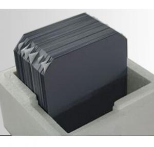
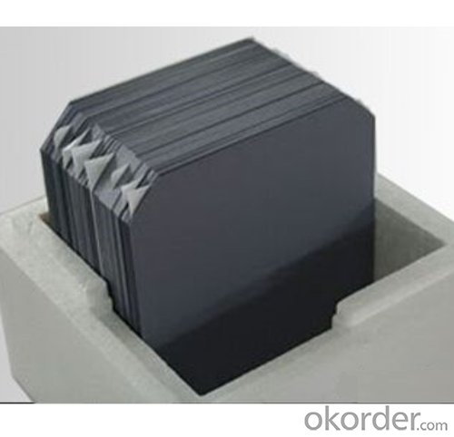
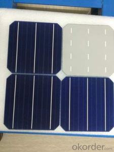
3. Solar Mono Silicon Wafer for Solar Cell (156 and 125) Images
")
")
4. Solar Mono Silicon Wafer for Solar Cell (156 and 125) Specification
窗体顶端 Item窗体底端 | N-type solar grade mono silicon wafer(125x125mm) | N-type solar grade mono silicon wafer(156x156mm) |
Growth Method | CZ | CZ |
Conductive Type | N-type | N-type |
Dopant | Phos. | Phos. |
Orientation | <100>±3° | <100>±3° |
Resistivity | 1 –3,3-6Ω•cm | 1 –3,3-6 Ω•cm |
Bulk Lifetime | ≥1000μs | ≥1000μs |
Oxygen Content | ≤0.1*1018 cm3 | ≤0.1*1018 cm3 |
Carbon Content | ≤0.1*1017 /cm3 | ≤0.1*1017 /cm3 |
Dimension | 125*125±0.5mm | 156*156±0.5mm |
Diagonal | 150±0.5mm | 200±0.5mm |
Square Sides Angle | 90±0.3° | 90±0.3° |
Thickness | 200±20 um | 200±20 um |
TTV | ≤25um | ≤25um |
Saw Mark | ≤15um | ≤15um |
Warp | ≤40um | ≤40um |
Chips | Depth<0.3mm;Length<0.5mm | Depth<0.3mm;Length<0.5mm, |
less than 2chips per wafer | less than 2chips per wafer | |
Appearance | No Stain, No Pinhole and Cracks by Visual Inspection | No Stain, No Pinhole and Cracks by Visual Inspection |
Dislocation Density | ≤1000 pcs/cm2 | ≤1000 pcs/cm2 |
Package | Packed in Polyethylene foam box,400pcs/box | Packed in Polyethylene foam box,400pcs/box 窗体底端 |
5. FAQ of Solar Mono Silicon Wafer for Solar Cell (156 and 125)
Q1. How long can we receive the product after purchase?
A1.In the purchase of product within three working days, We will arrange the factory delivery as soon as possible. The pecific time of receiving is related to the state and position of customers
Q2. Can we visit your factory?
A2:Surely, I will arrange the trip basing on your business schedule.
Q3:Which payment terms can you accept?
A3:T/T,L/C,Moneygram,Paypal are available for us.
- Q: How are solar silicon wafers connected in a series or parallel configuration?
- Solar silicon wafers are typically connected in a series configuration to increase the voltage output of the solar panel system. This means that the positive terminal of one wafer is connected to the negative terminal of the next wafer, resulting in an additive voltage. However, if the desired output is higher current, the wafers can be connected in a parallel configuration, where the positive terminals are connected together and the negative terminals are connected together, resulting in an additive current.
- Q: How are solar silicon wafers protected from external factors like moisture or dust?
- Solar silicon wafers are typically protected from external factors like moisture or dust by encapsulating them with a layer of protective materials. This encapsulation can be in the form of a glass or polymer coating, which acts as a barrier to prevent the entry of moisture or dust particles. Additionally, the solar cells are often sealed within a frame or module, further protecting them from external elements.
- Q: How are solar silicon wafers inspected for surface defects?
- Solar silicon wafers are inspected for surface defects using various techniques such as visual inspection, automated optical inspection (AOI), and scanning electron microscopy (SEM). Visual inspection involves examining the wafer surface under proper lighting conditions to identify any visible defects like cracks, scratches, or impurities. AOI utilizes high-resolution cameras and advanced algorithms to scan the wafer surface and detect any abnormalities or inconsistencies. SEM, on the other hand, provides a more detailed analysis by using electron beams to create high-resolution images of the wafer surface, enabling the identification of even smaller defects at a microscopic level. These inspection methods help ensure the quality and efficiency of solar silicon wafers in the production of solar cells.
- Q: Can solar silicon wafers be used in hybrid solar cell technologies?
- Yes, solar silicon wafers can be used in hybrid solar cell technologies. Hybrid solar cells combine different types of materials to optimize efficiency and performance. By incorporating silicon wafers along with other materials like organic polymers or perovskites, hybrid solar cells can harness a broader range of the solar spectrum and improve overall energy conversion.
- Q: Can solar silicon wafers be used in solar-powered desalination systems?
- Yes, solar silicon wafers can be used in solar-powered desalination systems. These wafers are commonly used to produce solar cells, which convert sunlight into electricity. By integrating solar silicon wafers into the desalination system, the generated electricity can power the process of removing salt and impurities from seawater, making it suitable for drinking or irrigation purposes.
- Q: What is the typical cost of a solar silicon wafer?
- The typical cost of a solar silicon wafer can vary depending on factors such as size, quality, and market conditions. However, on average, a solar silicon wafer can cost anywhere between $1 to $5 per wafer.
- Q: How is a spectral response measured in a solar silicon wafer?
- A spectral response in a solar silicon wafer is typically measured using a technique called external quantum efficiency (EQE) measurement. In this process, the wafer is illuminated with monochromatic light of varying wavelengths, and the resulting current generated by the solar cell is measured. The EQE measurement provides information about how efficiently the solar cell converts light of different wavelengths into electrical energy, allowing for a comprehensive understanding of the cell's spectral response.
- Q: How are solar silicon wafers tested for electrical performance?
- Solar silicon wafers are tested for electrical performance through a series of evaluations and measurements. This typically involves subjecting the wafers to various tests such as resistivity measurements, open-circuit voltage measurements, short-circuit current measurements, and efficiency calculations. These tests help assess the quality and efficiency of the solar cells produced from the wafers, ensuring they meet industry standards and perform optimally in converting sunlight into electricity.
- Q: Can solar silicon wafers be made transparent for specific applications?
- Yes, solar silicon wafers can be made transparent for specific applications by implementing various techniques such as thinning the wafer thickness, reducing crystal defects, and applying anti-reflective coatings. These measures allow a certain amount of light to pass through the wafer while maintaining its functionality as a solar cell. This transparency can be beneficial for applications like building-integrated photovoltaics (BIPV) or solar windows, where aesthetics and light transmission are important factors.
- Q: How are solar silicon wafers protected from thermal damage?
- Solar silicon wafers are protected from thermal damage through the implementation of various techniques. One common method is the use of anti-reflective coatings on the surface of the wafers, which helps to reduce the absorption of heat and minimize thermal stress. Additionally, some wafers are equipped with backside passivation layers that enhance their ability to dissipate heat. Moreover, proper packaging and installation of solar panels also play a crucial role in safeguarding the wafers from thermal damage by ensuring adequate heat dissipation and temperature control.
Send your message to us
Solar Mono Silicon Wafer for Solar Cell (156 and 125)
- Ref Price:
-
- Loading Port:
- China main port
- Payment Terms:
- TT or LC
- Min Order Qty:
- 10000 pc
- Supply Capability:
- 1000000 pc/month
OKorder Service Pledge
OKorder Financial Service
Similar products


Hot products


Hot Searches
Related keywords

