


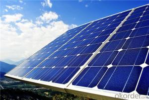
Silicon Wafer Solar - High Quality A Grade Polycrystalline 5V 16.2% Solar Cell
- Ref Price:
-

- Loading Port:
- Shanghai
- Payment Terms:
- TT OR LC
- Min Order Qty:
- 1000 pc
- Supply Capability:
- 100000 pc/month
OKorder Service Pledge
OKorder Financial Service
You Might Also Like


Specifications
hot sale solar cell
1.16.8%~18.25% high efficiency
2.100% checked quality
3.ISO9001/ISO14001/TUV/CE/UL
4.stable performance
We can offer you the best quality products and services, don't miss !
POLY6'(156*156)
Polycrystalline Silicon Solar cell
Physical Characteristics
Dimension: 156mm×156mm±0.5mm
Diagonal: 220mm±0.5mm
Thickness(Si): 200±20 μm
Front(-) Back(+)
Blue anti-reflecting coating (silicon nitride); Aluminum back surface field;
1.5mm wide bus bars; 2.0mm wide soldering pads;
Distance between bus bars: 51mm . Distance between bus bars :51mm .
Electrical Characteristics
Efficiency(%) | 18.00 | 17.80 | 17.60 | 17.40 | 17.20 | 16.80 | 16.60 | 16.40 | 16.20 | 16.00 | 15.80 | 15.60 |
Pmpp(W) | 4.33 | 4.29 | 4.24 | 4.19 | 4.14 | 4.09 | 4.04 | 3.99 | 3.94 | 3.90 | 3.86 | 3.82 |
Umpp(V) | 0.530 | 0.527 | 0.524 | 0.521 | 0.518 | 0.516 | 0.514 | 0.511 | 0.509 | 0.506 | 0.503 | 0.501 |
Impp(A) | 8.159 | 8.126 | 8.081 | 8.035 | 7.990 | 7.938 | 7.876 | 7.813 | 7.754 | 7.698 | 7.642 | 7.586 |
Uoc(V) | 0.633 | 0.631 | 0.628 | 0.625 | 0.623 | 0.620 | 0.618 | 0.617 | 0.615 | 0.613 | 0.611 | 0.609 |
Isc(A) | 8.709 | 8.677 | 8.629 | 8.578 | 8.531 | 8.478 | 8.419 | 8.356 | 8.289 | 8.220 | 8.151 | 8.083 |

MONO5'(125*125mm)165
Monocrystalline silicon solar cell
Physical Characteristics
Dimension: 125mm×125mm±0.5mm
Diagonal: 165mm±0.5mm
Thickness(Si): 200±20 μm
Front(-) Back(+)
Blue anti-reflecting coating(silicon nitride); Aluminum back surface field;
1.6mmwide bus bars; 2.5mm wide soldering pads;
Distance between bus bars: 61mm . Distance between bus bars :61mm .
Electrical Characteristics
Efficiency(%) | 19.40 | 19.20 | 19.00 | 18.80 | 18.60 | 18.40 | 18.20 | 18.00 | 17.80 | 17.60 | 17.40 | 17.20 |
Pmpp(W) | 2.97 | 2.94 | 2.91 | 2.88 | 2.85 | 2.82 | 2.79 | 2.76 | 2.73 | 2.70 | 2.67 | 2.62 |
Umpp(V) | 0.537 | 0.535 | 0.533 | 0.531 | 0.527 | 0.524 | 0.521 | 0.518 | 0.516 | 0.515 | 0.513 | 0.509 |
Impp(A) | 5.531 | 5.495 | 5.460 | 5.424 | 5.408 | 5.382 | 5.355 | 5.328 | 5.291 | 5.243 | 5.195 | 4.147 |
Uoc(V) | 0.637 | 0.637 | 0.636 | 0.635 | 0.633 | 0.630 | 0.629 | 0.629 | 0.628 | 0.626 | 0.626 | 0.625 |
Isc(A) | 5.888 | 5.876 | 5.862 | 5.848 | 5.839 | 5.826 | 5.809 | 5.791 | 5.779 | 5.756 | 5.293 | 5.144 |

FAQ:
Q:How can i get some sample?
A:Yes , if you want order ,sample is not a problem.
Q:How about your solar panel efficency?
A: Our product efficency around 17.25%~18.25%.
Q:What’s the certificate you have got?
A: we have overall product certificate of ISO9001/ISO14001/CE/TUV/UL
- Q: How do solar silicon wafers contribute to the overall efficiency of a solar panel?
- Solar silicon wafers are a crucial component of a solar panel as they play a significant role in enhancing its overall efficiency. These wafers are typically made from highly pure crystalline silicon, which is a semiconductor material capable of converting sunlight into electricity. By absorbing photons from sunlight, the silicon wafers generate an electric current that can be harnessed for various applications. The design and quality of these wafers heavily influence the efficiency of solar panels, as they determine how effectively sunlight is converted into electrical energy. Higher quality silicon wafers with fewer impurities and defects ensure better light absorption and enhanced electron mobility, resulting in improved conversion rates and overall efficiency of the solar panel.
- Q: Can solar silicon wafers be used in solar-powered irrigation systems?
- Yes, solar silicon wafers can be used in solar-powered irrigation systems. Solar silicon wafers are commonly used in the production of solar panels, which generate electricity from sunlight. This electricity can power irrigation systems, including pumps and sprinklers, enabling the efficient and sustainable use of water resources in agricultural practices.
- Q: Can solar silicon wafers be used in solar-powered space vehicles?
- Yes, solar silicon wafers can be used in solar-powered space vehicles. They are commonly used in photovoltaic cells to convert sunlight into electricity, providing a sustainable power source for space missions.
- Q: Are solar silicon wafers affected by chemical exposure?
- Yes, solar silicon wafers can be affected by chemical exposure. Chemicals, such as certain acids or solvents, can corrode or etch the surface of the wafers, leading to reduced efficiency or even failure of the solar cells. It is important to handle and store solar silicon wafers properly to avoid chemical damage.
- Q: How is a front contact applied to a solar silicon wafer?
- A front contact is typically applied to a solar silicon wafer using a screen printing process. The process involves depositing a conductive paste onto the front surface of the wafer through a fine mesh screen. This paste consists of metal particles, such as silver or aluminum, mixed with a binder material. The screen is aligned with the wafer's surface, and the paste is forced through the screen using a squeegee, leaving a patterned layer of conductive material on the wafer. This front contact layer helps to collect and transport the electrical current generated by the solar cells.
- Q: What is the role of surface passivation layers on solar silicon wafers?
- The role of surface passivation layers on solar silicon wafers is to minimize the recombination of charge carriers, such as electrons and holes, at the surface of the wafer. These layers help improve the efficiency and performance of solar cells by reducing surface recombination losses, increasing the lifetime of charge carriers, and enhancing the overall electrical properties of the device.
- Q: Are solar silicon wafers affected by power outages?
- No, solar silicon wafers are not directly affected by power outages since they do not rely on external power sources. They generate electricity from sunlight by converting photons into electrons, without the need for an active power supply. However, during a power outage, the solar panels themselves will not produce electricity unless they are connected to a functioning grid or have an energy storage system like batteries in place.
- Q: What is the impact of impurities on the efficiency of solar silicon wafers?
- Impurities can significantly impact the efficiency of solar silicon wafers. The presence of impurities like boron or phosphorous can alter the electrical properties of the silicon, affecting its ability to convert sunlight into electricity. These impurities can introduce defects in the crystal lattice, leading to a decrease in the wafer's overall performance. Additionally, impurities can also interfere with the formation of essential junctions within the wafer, further reducing its efficiency. Therefore, minimizing impurities during the manufacturing process is crucial to ensure optimal performance and maximum energy conversion in solar silicon wafers.
- Q: How are solar silicon wafers affected by dust or dirt accumulation?
- Solar silicon wafers are negatively affected by dust or dirt accumulation as it can reduce their efficiency in capturing sunlight. The accumulation of dust or dirt on the surface of the wafers creates a barrier that prevents sunlight from reaching the silicon, therefore reducing the amount of energy that can be converted into electricity. This accumulation can decrease the overall performance of solar panels and may require regular cleaning to maintain optimal efficiency.
- Q: Can solar silicon wafers be used in water desalination plants?
- Yes, solar silicon wafers can be used in water desalination plants. They can be utilized as a component in solar panels to generate electricity, which can then be used to power the desalination process.
Send your message to us
Silicon Wafer Solar - High Quality A Grade Polycrystalline 5V 16.2% Solar Cell
- Ref Price:
-
- Loading Port:
- Shanghai
- Payment Terms:
- TT OR LC
- Min Order Qty:
- 1000 pc
- Supply Capability:
- 100000 pc/month
OKorder Service Pledge
OKorder Financial Service
Similar products


Hot products


Hot Searches
Related keywords

