


High Quality A Grade Monocrystalline Solar Grade Silicon Wafer Polycrystalline 5v 17.2% Solar Cell
- Ref Price:
-

- Loading Port:
- Shanghai
- Payment Terms:
- TT OR LC
- Min Order Qty:
- 1000 pc
- Supply Capability:
- 100000 pc/month
OKorder Service Pledge
OKorder Financial Service
You Might Also Like


Specifications
hot sale solar cell
1.16.8%~18.25% high efficiency
2.100% checked quality
3.ISO9001/ISO14001/TUV/CE/UL
4.stable performance
We can offer you the best quality products and services, don't miss !
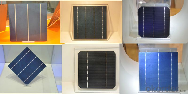
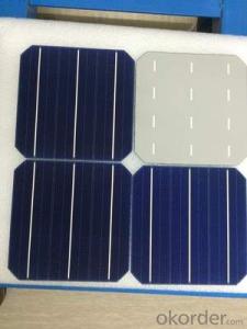
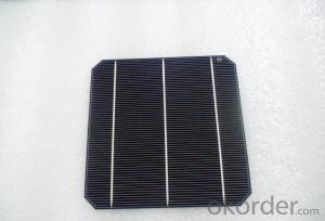
POLY6'(156*156)
Polycrystalline Silicon Solar cell
Physical Characteristics
Dimension: 156mm×156mm±0.5mm
Diagonal: 220mm±0.5mm
Thickness(Si): 200±20 μm
Front(-) Back(+)
Blue anti-reflecting coating (silicon nitride); Aluminum back surface field;
1.5mm wide bus bars; 2.0mm wide soldering pads;
Distance between bus bars: 51mm . Distance between bus bars :51mm .
Electrical Characteristics
Efficiency(%) | 18.00 | 17.80 | 17.60 | 17.40 | 17.20 | 16.80 | 16.60 | 16.40 | 16.20 | 16.00 | 15.80 | 15.60 |
Pmpp(W) | 4.33 | 4.29 | 4.24 | 4.19 | 4.14 | 4.09 | 4.04 | 3.99 | 3.94 | 3.90 | 3.86 | 3.82 |
Umpp(V) | 0.530 | 0.527 | 0.524 | 0.521 | 0.518 | 0.516 | 0.514 | 0.511 | 0.509 | 0.506 | 0.503 | 0.501 |
Impp(A) | 8.159 | 8.126 | 8.081 | 8.035 | 7.990 | 7.938 | 7.876 | 7.813 | 7.754 | 7.698 | 7.642 | 7.586 |
Uoc(V) | 0.633 | 0.631 | 0.628 | 0.625 | 0.623 | 0.620 | 0.618 | 0.617 | 0.615 | 0.613 | 0.611 | 0.609 |
Isc(A) | 8.709 | 8.677 | 8.629 | 8.578 | 8.531 | 8.478 | 8.419 | 8.356 | 8.289 | 8.220 | 8.151 | 8.083 |

MONO5'(125*125mm)165
Monocrystalline silicon solar cell
Physical Characteristics
Dimension: 125mm×125mm±0.5mm
Diagonal: 165mm±0.5mm
Thickness(Si): 200±20 μm
Front(-) Back(+)
Blue anti-reflecting coating(silicon nitride); Aluminum back surface field;
1.6mmwide bus bars; 2.5mm wide soldering pads;
Distance between bus bars: 61mm . Distance between bus bars :61mm .
Electrical Characteristics
Efficiency(%) | 19.40 | 19.20 | 19.00 | 18.80 | 18.60 | 18.40 | 18.20 | 18.00 | 17.80 | 17.60 | 17.40 | 17.20 |
Pmpp(W) | 2.97 | 2.94 | 2.91 | 2.88 | 2.85 | 2.82 | 2.79 | 2.76 | 2.73 | 2.70 | 2.67 | 2.62 |
Umpp(V) | 0.537 | 0.535 | 0.533 | 0.531 | 0.527 | 0.524 | 0.521 | 0.518 | 0.516 | 0.515 | 0.513 | 0.509 |
Impp(A) | 5.531 | 5.495 | 5.460 | 5.424 | 5.408 | 5.382 | 5.355 | 5.328 | 5.291 | 5.243 | 5.195 | 4.147 |
Uoc(V) | 0.637 | 0.637 | 0.636 | 0.635 | 0.633 | 0.630 | 0.629 | 0.629 | 0.628 | 0.626 | 0.626 | 0.625 |
Isc(A) | 5.888 | 5.876 | 5.862 | 5.848 | 5.839 | 5.826 | 5.809 | 5.791 | 5.779 | 5.756 | 5.293 | 5.144 |

FAQ:
Q:How can i get some sample?
A:Yes , if you want order ,sample is not a problem.
Q:How about your solar panel efficency?
A: Our product efficency around 17.25%~18.25%.
Q:What’s the certificate you have got?
A: we have overall product certificate of ISO9001/ISO14001/CE/TUV/UL
- Q: Can solar silicon wafers be used in solar-powered boats?
- Yes, solar silicon wafers can be used in solar-powered boats. These wafers are commonly used in solar panels to convert sunlight into electricity, which can power various systems including propulsion in solar-powered boats.
- Q: How is the surface of a solar silicon wafer textured?
- The surface of a solar silicon wafer is textured by using various techniques such as acid etching or laser ablation. These methods create a pattern of tiny pyramidal or needle-like structures on the surface, which helps to trap and scatter light, increasing the absorption efficiency of the silicon wafer.
- Q: What is the purpose of a degradation rate in a solar silicon wafer?
- The purpose of a degradation rate in a solar silicon wafer is to measure and quantify the rate at which the performance of the wafer decreases over time due to various factors such as aging, exposure to environmental conditions, and mechanical stress. This degradation rate helps in understanding the long-term reliability and durability of the wafer, and aids in predicting its lifespan and overall efficiency in generating solar power.
- Q: How thick is a solar silicon wafer?
- A solar silicon wafer is typically around 180-200 micrometers thick.
- Q: How are solar silicon wafers protected from theft or unauthorized use?
- Solar silicon wafers are typically protected from theft or unauthorized use through various security measures. These can include physical security measures such as restricted access to manufacturing facilities and storage areas, surveillance systems, and alarm systems. Additionally, strict inventory control and tracking systems are implemented to ensure that each wafer is accounted for and can be traced back to its origin. These measures help deter theft and unauthorized use, ensuring the security and integrity of solar silicon wafers.
- Q: How are solar silicon wafers affected by photon recycling?
- Solar silicon wafers are positively affected by photon recycling as it allows for the reabsorption and redirection of unused photons within the solar cell, increasing overall efficiency.
- Q: Can solar silicon wafers be used in disaster relief efforts?
- Yes, solar silicon wafers can be used in disaster relief efforts. They can provide a reliable source of renewable energy in areas where the conventional power grid may be damaged or non-existent after a disaster. Solar panels, made with silicon wafers, can generate electricity to power emergency communication systems, medical equipment, lighting, and other essential devices, aiding relief operations and improving living conditions for affected communities.
- Q: How do solar silicon wafers contribute to the circular economy?
- Solar silicon wafers contribute to the circular economy by enabling the production of renewable energy through solar panels. As a key component of solar cells, silicon wafers help harness the power of the sun and convert it into electricity. By using solar energy, we reduce our reliance on fossil fuels, decrease greenhouse gas emissions, and promote sustainability. Additionally, the recycling and reusing of silicon wafers help minimize waste and conserve valuable resources, making them an essential element in the circular economy.
- Q: What is the effect of surface roughness on solar silicon wafers?
- The effect of surface roughness on solar silicon wafers is twofold. Firstly, it can enhance light trapping, increasing the absorption of sunlight and consequently improving the efficiency of the solar cells. Secondly, excessive surface roughness can lead to increased recombination of charge carriers, reducing the overall performance of the solar cells. Therefore, achieving an optimal level of surface roughness is crucial for maximizing the efficiency of solar silicon wafers.
- Q: Specific kind of industry to use the reference price is what?!I have a ton of silicon chips, want to sell, do not know what the price, do not know what the company needs!
- Affected by the rapid growth of demand for solar energy, the production of silicon raw material polysilicon prices a few years up to 3 times, and is expected in the next few years, polysilicon supply gap will be maintained at around 5000 tons, the price of polysilicon is expected to continue to rise. This will likely lead to a new round of China's silicon chip industry reshuffle, looking for international technology partners will be one of the ways.Photovoltaic industry to promote polysilicon prices skyrocketingPhotovoltaic industry is becoming the hottest new energy industry, the United States listed Wuxi Suntech chairman Shi Zhengrong thus became one of the richest people in china. But the vigorous development of solar cells also led to rising prices of polysilicon raw materials, and hit the domestic semiconductor materials industry.
Send your message to us
High Quality A Grade Monocrystalline Solar Grade Silicon Wafer Polycrystalline 5v 17.2% Solar Cell
- Ref Price:
-
- Loading Port:
- Shanghai
- Payment Terms:
- TT OR LC
- Min Order Qty:
- 1000 pc
- Supply Capability:
- 100000 pc/month
OKorder Service Pledge
OKorder Financial Service
Similar products


Hot products


Hot Searches
Related keywords

