


Monocrystalline Solar Grade Silicon Wafer - Mono Solar Cells 156mm*156mm in Bulk Quantity Low Price Stock 18.2
- Ref Price:
-

- Loading Port:
- Shanghai
- Payment Terms:
- TT OR LC
- Min Order Qty:
- 1000 pc
- Supply Capability:
- 100000 pc/month
OKorder Service Pledge
OKorder Financial Service
You Might Also Like


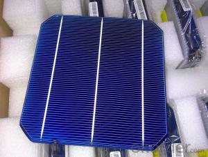
Brief Introduction
- Up to 20.0% efficiency, one of the highest performing mono crystalline cells on the market
- Three bus bars boosts current collection over the entire cell area, leading to higher fill factors
- Blue anti-reflecting coating allows more sunlight be captured and converted to electricity
- Finer, closer fingers improves charge collections for improved energy yield
- Lower light-induced degradation leads to greater power output over the entire module lifetime
- All solar cells are tightly classified to optimize output of module
- Maximum yield and longevity due to hotspot prevention
- Premium appearance results in a highly uniform and aesthetically appealing module
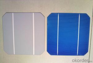
Specification
- Product Mono-crystalline silicon solar cell
- Dimension 156 mm x 156 mm ± 0.5 mm
- Thickness 200 μm ± 30 μm
- Front 1.5 ± 0.1 mm busbar (silver)
- Silicon nitride antireflection coating
- Back 3.0 mm continuous soldering pads (silver)
- Back surface field (aluminum)
Electric performance parameters

- Testing conditions: 1000 W/m2, AM 1.5, 25 °C, Tolerance: Efficiency ± 0.2% abs., Pmpp ±1.5% rel.
- Imin : at 0.5 V
Light Intensity Dependence

Soldering Ability
- Peel Strength: > 1.0 N/mm (Pull soldered ribbon from busbar in 5 mm/s of 180°)
Dimension Figure

Quick Response
- Any time and anywhere, reply clients' email and solve all problems happen in the work at the first time.
- Remove clients doubts and offer the best solution at the first time.
- Give our clients the lastest news of the photovoltaic, update the newest stock informtion.
Production and Quality Control
- Precision cell efficiency sorting procedures
- Stringent criteria for color uniformity and appearance
- Reverse current and shunt resistance screening
- ISO9001,ISO14001 and OHSAS 18001,TUV Certificated


FAQ:
1. Q: Do you have your own factory?
A: Yes, we have. Our factory located in Jiangsu
2. Q: How can I visit your factory?
A: Before you visit,please contact us.We will show you the route or arrange a car to pick you up.
3. Q: Do you provide free sample?
A: Commenly we provide paid sample.
4. Q: Could you print our company LOGO on the nameplate and package?
A: Yes, we accept it.And need an Authorization Letter from you.
5. Q: Do you accept custom design on size?
A: Yes, if the size is reasonable.
6. Q: How can I be your agent in my country?
A: Please leave feedback. It's better for us to talk about details by email.
7. Q: Do you have solar project engineer who can guide me to install system?
A: Yes, we have a professional engineer team. They can teach you how to install a solar system.
- Q: What is the typical purity level of silicon used in solar silicon wafers?
- The typical purity level of silicon used in solar silicon wafers is around 99.9999%, also known as 6N purity.
- Q: What are the reasons for the emergence of the black chip phenomenon of the monocrystalline silicon, which aspects of the production process have an impact on it, preventive measures, and improvement measures?
- You say the phenomenon called flower piece, the formation of many factors, the main reason is that contamination, because in the process, the wafer surface after polishing the silicon atom is bond breaking, it is easy to adsorb metal ions and cannot completely by cleaning out.
- Q: Are there any limitations to using solar silicon wafers in solar cells?
- Yes, there are several limitations to using solar silicon wafers in solar cells. One limitation is the high cost of producing silicon wafers, making solar cells more expensive compared to other energy sources. Additionally, silicon wafers are rigid and bulky, which limits their application in certain solar cell designs. Another limitation is the efficiency of silicon-based solar cells, as they have lower conversion efficiencies compared to emerging solar technologies like thin-film solar cells. Furthermore, the production of silicon wafers requires a significant amount of energy, contributing to the carbon footprint of solar cell manufacturing. Overall, while silicon wafers are widely used, their limitations highlight the need for ongoing research and development to enhance solar cell technologies.
- Q: Can solar silicon wafers be used in hybrid solar systems?
- Yes, solar silicon wafers can definitely be used in hybrid solar systems. Hybrid solar systems combine multiple sources of energy generation, such as solar, wind, or battery storage, to optimize energy production and ensure a continuous power supply. Solar silicon wafers are the key component in solar panels used to harness solar energy, making them an integral part of hybrid solar systems.
- Q: Process flow of wafer wafer ultrasonic cleaning machine?
- Plasma wafer cleaning parameters:Residual plasma cleaning method of particles 1, silicon wafer surface, which comprises the following steps: firstly, gas flushing process, and then the gas plasma glow; the use of either gas from the 02, Ar, N2; gas washing process parameters set process: the chamber pressure of 10-40 mTorr, process gas flow 100-500sccm time, 1-5s; process parameters of starting process is: the chamber pressure of 1040 mTorr, process gas flow on the electrode 100-500sccm, power 250-400W, time 1-10s.2, as described in the plasma cleaning method, the invention is characterized in that the gas used is 23, plasma cleaning method, which is characterized in that the process parameters of gas flushing process is: the chamber pressure of 15 mTorr, process gas flow 300sccm, time 3S; process parameters of starting process is: the chamber pressure of 15 mTorr, process gas flow on the electrode 300sccm, power 300W, time Ss.4, plasma cleaning method, which is characterized in that the process parameters of gas flushing process is: the chamber pressure of 10-20 mTorr, process gas flow 100-300sccm, time 1-5s; process parameters of starting process is: the chamber pressure of 10-20 mTorr, process gas flow on the electrode 100-300sccm, power 250-400W, when Lu 1-5s.
- Q: Can solar silicon wafers be used in wearable fashion accessories?
- Yes, solar silicon wafers can be used in wearable fashion accessories. They can be integrated into various accessories like jewelry, clothing, or accessories such as bags and hats to harness solar energy for charging devices or powering other functionalities.
- Q: Why do they make so many transistors on silicon in an integrated circuit
- For digital integrated circuits, mainly used for logic operations, and, or, not by the most basic logic constitute a complex logic. Computers are now so complex that they require a lot of transistors.For analog integrated circuits, mainly used to amplify the signal, such as your phone Wifi and other received signals are very weak, you want to use transistor amplifier.
- Q: How are solar silicon wafers affected by light trapping techniques?
- Solar silicon wafers are positively affected by light trapping techniques as they enhance the absorption of sunlight and increase the overall efficiency of the solar cell. These techniques, such as textured surfaces or nanostructures, help to trap light within the wafer by increasing the path length of the photons, allowing for more chances of absorption and reducing reflection. This leads to improved light absorption and higher conversion of sunlight into electricity, making the solar cells more effective and efficient.
- Q: What are the different materials used for front contacts in solar silicon wafers?
- The different materials used for front contacts in solar silicon wafers include silver (Ag), aluminum (Al), and copper (Cu). These materials are commonly used for their high conductivity and durability, allowing efficient electron collection and minimizing resistive losses in photovoltaic cells.
- Q: How do solar silicon wafers handle extreme temperatures?
- Solar silicon wafers are designed to handle extreme temperatures quite well. They are typically made from high-grade silicon materials that can withstand both very high and low temperatures. The silicon material has a high melting point and excellent thermal stability, allowing it to handle the heat generated from sunlight and the surrounding environment. Additionally, solar cells are often encapsulated with protective layers and materials that provide further insulation and temperature resistance. This ensures that solar silicon wafers can continue to generate electricity efficiently, even in extreme temperature conditions.
Send your message to us
Monocrystalline Solar Grade Silicon Wafer - Mono Solar Cells 156mm*156mm in Bulk Quantity Low Price Stock 18.2
- Ref Price:
-
- Loading Port:
- Shanghai
- Payment Terms:
- TT OR LC
- Min Order Qty:
- 1000 pc
- Supply Capability:
- 100000 pc/month
OKorder Service Pledge
OKorder Financial Service
Similar products


Hot products


Hot Searches
Related keywords

