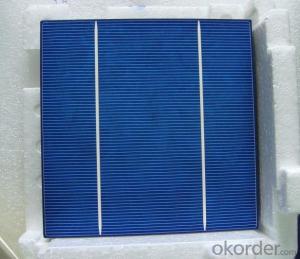
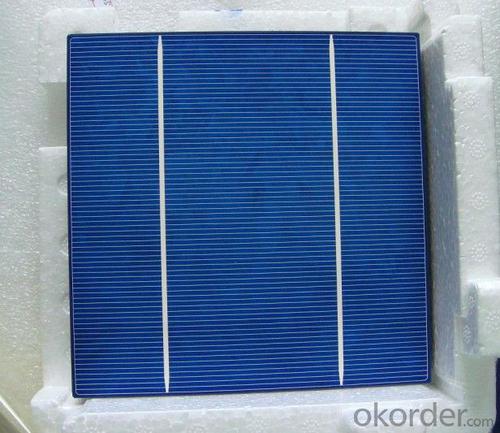


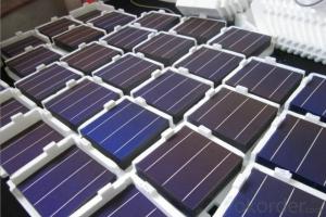
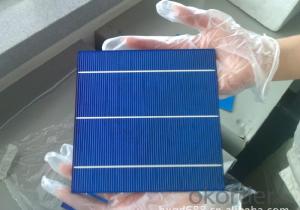
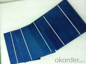
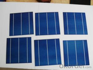
A Silicon Wafer Solar Cell - High Current 18.2% Polycrystalline Silicon Solar Cell
- Ref Price:
-

- Loading Port:
- Shanghai
- Payment Terms:
- TT OR LC
- Min Order Qty:
- 1000 pc
- Supply Capability:
- 100000 pc/month
OKorder Service Pledge
OKorder Financial Service
You Might Also Like


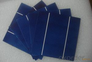
4 Bus Bars 156*156 17.6% efficiency poly solar cell
PHYSICAL CHARACTERISTICS
Dimension: 156mm x 156mm ± 0.5mm
Wafer Thickeness: 180um+20um and 200um+20um
Front(-) Four 1.2mm silver busbar
Silicon nitride blue anti-reflection coating
Back(+) aluminum back surface field
1.75mm(silver) wide segment soldering pads

Typical Electrical Characteristics
Efficiency | W(Pmpp) | V(Umpp) | A(Impp) | V(Uoc) | A(Isc) |
17.4-17.5 | 4.234 | 0.517 | 8.231 | 0.622 | 8.759 |
17.5-17.6 | 4.259 | 0.519 | 8.243 | 0.623 | 8.769 |
17.7-17.8 | 4.283 | 0.521 | 8.256 | 0.625 | 8.779 |
17.8-17.9 | 4.307 | 0.523 | 8.268 | 0.626 | 8.788 |
17.9-18.0 | 4.332 | 0.525 | 8.281 | 0.627 | 8.798 |
18.0-18.1 | 4.380 | 0.529 | 8.306 | 0.629 | 8.808 |
18.1-18.2 | 4.405 | 0.531 | 8.318 | 0.632 | 8.818 |
18.2-18.3 | 4.429 | 0.533 | 8.331 | 0.633 | 8.837 |
18.3-18.4 | 4.453 | 0.535 | 8.344 | 0.634 | 8.847 |
18.4-18.5 | 4.478 | 0.537 | 8.356 | 0.636 | 8.856 |
18.5-18.6 | 4.502 | 0.539 | 8.369 | 0.637 | 8.866 |
Efficiency | W(Pmpp) | V(Umpp) | A(Impp) | V(Uoc) | A(Isc) |
20.90-21.00 | 5.06 | 0.557 | 9.007 | 0.653 | 9.688 |
20.80-20.90 | 5.04 | 0.556 | 9.062 | 0.652 | 9.683 |
20.70-20.80 | 5.02 | 0.554 | 9.055 | 0.651 | 9.684 |
20.60-20.70 | 4.99 | 0.552 | 9.033 | 0.651 | 9.672 |
20.50-20.60 | 4.97 | 0.550 | 9.002 | 0.650 | 9.673 |
20.40-20.50 | 4.94 | 0.548 | 9.012 | 0.649 | 9.674 |
20.30-20.40 | 4.92 | 0.546 | 9.009 | 0.649 | 9.655 |
20.20-20.30 | 4.89 | 0.543 | 9.012 | 0.648 | 9.634 |
20.10-20.20 | 4.87 | 0.541 | 8.998 | 0.648 | 9.617 |
20.00-20.10 | 4.85 | 0.540 | 8.977 | 0.647 | 9.600 |
*Data under standard testing conditional (STC):1,000w/m2,AM1.5, 25°C , Pmax:Positive power tolerance.
3 Bus Bars 156*156 17.4% efficiency poly solar cell
Dimension: 156 mm x 156 mm ± 0.5 mm
Wafer Thickeness: 156 mm x 156 mm ± 0.5 mm

Typical Electrical Characteristics:
| Efficiency code | 1660 | 1680 | 1700 | 1720 | 1740 | 1760 | 1780 | 1800 | 1820 | 1840 | 1860 |
| Efficiency (%) | 16.6 | 16.8 | 17.0 | 17.2 | 17.4 | 17.6 | 17.8 | 18.0 | 18.2 | 18.4 | 18.6 |
| Pmax (W) | 4.04 | 4.09 | 4.14 | 4.19 | 4.23 | 4.28 | 4.33 | 4.38 | 4.43 | 4.48 | 4.53 |
| Voc (V) | 0.612 | 0.615 | 0.618 | 0.621 | 0.624 | 0.627 | 0.629 | 0.63 | 0.633 | 0.635 | 0.637 |
| Isc (A) | 8.42 | 8.46 | 8.51 | 8.56 | 8.61 | 8.65 | 8.69 | 8.73 | 8.77 | 8.81 | 8.84 |
| Imp (A) | 7.91 | 7.99 | 8.08 | 8.16 | 8.22 | 8.27 | 8.33 | 8.38 | 8.43 | 8.48 | 8.53 |
* Testing conditions: 1000 W/m2, AM 1.5, 25 °C, Tolerance: Efficiency ± 0.2% abs., Pmpp ±1.5% rel.
* Imin : at 0.5 V
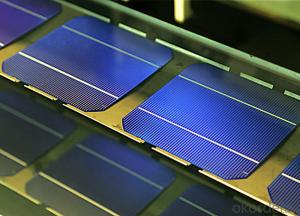
Production:

Package:

FAQ:
1. Q: Do you have your own factory?
A: Yes, we have. Our factory located in Jiangsu
2. Q: How can I visit your factory?
A: Before you visit,please contact us.We will show you the route or arrange a car to pick you up.
3. Q: Do you provide free sample?
A: Commenly we provide paid sample.
4. Q: Could you print our company LOGO on the nameplate and package?
A: Yes, we accept it.And need an Authorization Letter from you.
5. Q: Do you accept custom design on size?
A: Yes, if the size is reasonable.
6. Q: How can I be your agent in my country?
A: Please leave feedback. It's better for us to talk about details by email.
7. Q: Do you have solar project engineer who can guide me to install system?
A: Yes, we have a professional engineer team. They can teach you how to install a solar system.
- Q: How are solar silicon wafers handled and transported?
- Solar silicon wafers are handled and transported with great care to ensure their quality and integrity. They are typically stored in cleanroom environments to prevent contamination. When being transported, they are usually packaged in protective materials such as antistatic bags or foam inserts to prevent any damage or breakage. Specialized carriers or trucks equipped with shock-absorbing systems are used to minimize vibrations and impacts during transportation. Additionally, temperature and humidity control measures are implemented to avoid any adverse effects on the wafers. Overall, meticulous handling and secure packaging are essential to maintain the high quality of solar silicon wafers throughout their transportation process.
- Q: Can solar silicon wafers be used in solar water heating systems?
- Yes, solar silicon wafers can be used in solar water heating systems. These wafers are typically used in photovoltaic solar panels to convert sunlight into electricity. However, they can also be utilized in solar water heating systems to help capture and transfer solar energy to heat water.
- Q: How are solar silicon wafers protected from bird droppings?
- Solar silicon wafers are typically protected from bird droppings through the use of anti-reflective coatings, which make the surface less attractive for birds to perch on. Additionally, some solar installations may utilize bird deterrents such as netting or spikes to prevent birds from landing and potentially causing damage or soiling the wafers.
- Q: I work in a solar cell company, do silicon chip testing on the human body what chronic harm?
- If it is at least module, such as CVD PVD, there are some toxic gases
- Q: How do solar silicon wafers perform in low-temperature environments?
- Solar silicon wafers generally perform well in low-temperature environments. However, their efficiency tends to decrease as the temperature drops. This is because the electrical resistance of the silicon material increases in colder temperatures, leading to a reduction in power output. Additionally, extreme cold can cause thermal stresses on the wafers, potentially leading to cracking or damage. Therefore, while solar silicon wafers can still generate electricity in low-temperature conditions, their overall performance may be slightly compromised compared to optimal operating temperatures.
- Q: Can solar silicon wafers be used in off-grid systems?
- Yes, solar silicon wafers can be used in off-grid systems. Solar silicon wafers are the key component in photovoltaic cells, which generate electricity from sunlight. Off-grid systems rely on generating electricity independently, without connecting to the main power grid. Solar silicon wafers, when integrated into solar panels, can capture sunlight and convert it into electrical energy, making them suitable for off-grid applications where no grid connection is available or desired.
- Q: What is the purpose of a spectral response in a solar silicon wafer?
- The purpose of a spectral response in a solar silicon wafer is to measure and understand how the wafer responds to different wavelengths of light. This information is crucial in determining the efficiency and performance of the solar cell, as it helps in identifying the parts of the solar spectrum that the cell can effectively convert into electricity.
- Q: How are solar silicon wafers protected from handling-induced microcracks?
- Solar silicon wafers are protected from handling-induced microcracks through several measures. Firstly, they are usually coated with a thin layer of protective material, such as a polymer film or glass, which serves as a physical barrier against potential damage during handling. Additionally, manufacturers employ advanced manufacturing techniques to strengthen the wafer's structure, making it more resistant to microcracks. These techniques may include doping the silicon with specific impurities or applying stress-reducing treatments. Finally, strict handling protocols are implemented, ensuring that the wafers are carefully transported and manipulated to minimize the risk of microcracks.
- Q: Can solar silicon wafers be used in solar-powered telecommunications systems?
- Yes, solar silicon wafers can be used in solar-powered telecommunications systems. These wafers are typically used to manufacture solar cells, which convert sunlight into electricity. By utilizing solar silicon wafers, telecommunications systems can harness solar energy to power their operations, reducing their reliance on traditional energy sources and promoting sustainability.
- Q: What is the role of solar silicon wafers in the overall solar energy system?
- Solar silicon wafers are a crucial component of the overall solar energy system as they serve as the building blocks for solar cells. These wafers are made from highly purified silicon and are responsible for converting sunlight into electricity through the photovoltaic process. By absorbing photons from the sun, the silicon wafers generate an electric current, which is then harnessed and utilized in various applications. Ultimately, the role of solar silicon wafers is to enable the efficient and sustainable production of solar energy, making them an essential element in the broader solar energy system.
Send your message to us
A Silicon Wafer Solar Cell - High Current 18.2% Polycrystalline Silicon Solar Cell
- Ref Price:
-
- Loading Port:
- Shanghai
- Payment Terms:
- TT OR LC
- Min Order Qty:
- 1000 pc
- Supply Capability:
- 100000 pc/month
OKorder Service Pledge
OKorder Financial Service
Similar products


Hot products


Hot Searches
Related keywords

