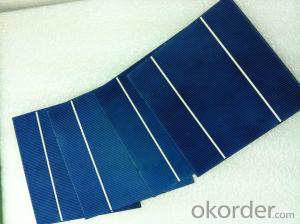
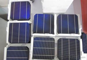
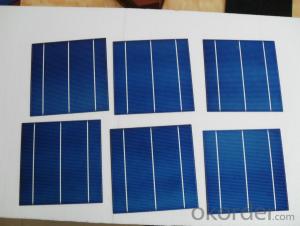
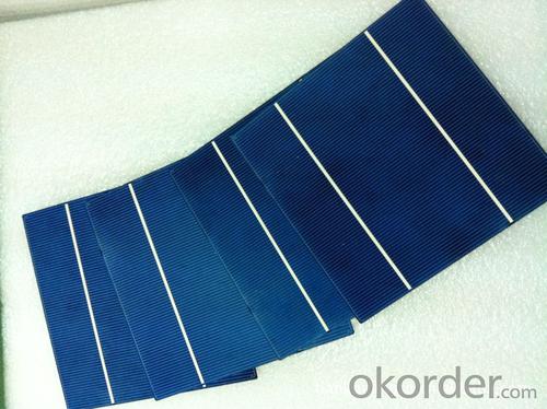


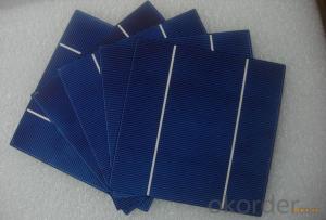
Solar Silicon Wafer Cassette Compatible High Current 17.2% Polycrystalline Silicon Solar Cell
- Ref Price:
-

- Loading Port:
- Shanghai
- Payment Terms:
- TT OR LC
- Min Order Qty:
- 1000 pc
- Supply Capability:
- 100000 pc/month
OKorder Service Pledge
OKorder Financial Service
You Might Also Like


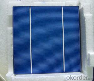
4 Bus Bars 156*156 17.6% efficiency poly solar cell
PHYSICAL CHARACTERISTICS
Dimension: 156mm x 156mm ± 0.5mm
Wafer Thickeness: 180um+20um and 200um+20um
Front(-) Four 1.2mm silver busbar
Silicon nitride blue anti-reflection coating
Back(+) aluminum back surface field
1.75mm(silver) wide segment soldering pads

Typical Electrical Characteristics
Efficiency | W(Pmpp) | V(Umpp) | A(Impp) | V(Uoc) | A(Isc) |
17.4-17.5 | 4.234 | 0.517 | 8.231 | 0.622 | 8.759 |
17.5-17.6 | 4.259 | 0.519 | 8.243 | 0.623 | 8.769 |
17.7-17.8 | 4.283 | 0.521 | 8.256 | 0.625 | 8.779 |
17.8-17.9 | 4.307 | 0.523 | 8.268 | 0.626 | 8.788 |
17.9-18.0 | 4.332 | 0.525 | 8.281 | 0.627 | 8.798 |
18.0-18.1 | 4.380 | 0.529 | 8.306 | 0.629 | 8.808 |
18.1-18.2 | 4.405 | 0.531 | 8.318 | 0.632 | 8.818 |
18.2-18.3 | 4.429 | 0.533 | 8.331 | 0.633 | 8.837 |
18.3-18.4 | 4.453 | 0.535 | 8.344 | 0.634 | 8.847 |
18.4-18.5 | 4.478 | 0.537 | 8.356 | 0.636 | 8.856 |
18.5-18.6 | 4.502 | 0.539 | 8.369 | 0.637 | 8.866 |
Efficiency | W(Pmpp) | V(Umpp) | A(Impp) | V(Uoc) | A(Isc) |
20.90-21.00 | 5.06 | 0.557 | 9.007 | 0.653 | 9.688 |
20.80-20.90 | 5.04 | 0.556 | 9.062 | 0.652 | 9.683 |
20.70-20.80 | 5.02 | 0.554 | 9.055 | 0.651 | 9.684 |
20.60-20.70 | 4.99 | 0.552 | 9.033 | 0.651 | 9.672 |
20.50-20.60 | 4.97 | 0.550 | 9.002 | 0.650 | 9.673 |
20.40-20.50 | 4.94 | 0.548 | 9.012 | 0.649 | 9.674 |
20.30-20.40 | 4.92 | 0.546 | 9.009 | 0.649 | 9.655 |
20.20-20.30 | 4.89 | 0.543 | 9.012 | 0.648 | 9.634 |
20.10-20.20 | 4.87 | 0.541 | 8.998 | 0.648 | 9.617 |
20.00-20.10 | 4.85 | 0.540 | 8.977 | 0.647 | 9.600 |
*Data under standard testing conditional (STC):1,000w/m2,AM1.5, 25°C , Pmax:Positive power tolerance.
3 Bus Bars 156*156 17.4% efficiency poly solar cell
Dimension: 156 mm x 156 mm ± 0.5 mm
Wafer Thickeness: 156 mm x 156 mm ± 0.5 mm

Typical Electrical Characteristics:
| Efficiency code | 1660 | 1680 | 1700 | 1720 | 1740 | 1760 | 1780 | 1800 | 1820 | 1840 | 1860 |
| Efficiency (%) | 16.6 | 16.8 | 17.0 | 17.2 | 17.4 | 17.6 | 17.8 | 18.0 | 18.2 | 18.4 | 18.6 |
| Pmax (W) | 4.04 | 4.09 | 4.14 | 4.19 | 4.23 | 4.28 | 4.33 | 4.38 | 4.43 | 4.48 | 4.53 |
| Voc (V) | 0.612 | 0.615 | 0.618 | 0.621 | 0.624 | 0.627 | 0.629 | 0.63 | 0.633 | 0.635 | 0.637 |
| Isc (A) | 8.42 | 8.46 | 8.51 | 8.56 | 8.61 | 8.65 | 8.69 | 8.73 | 8.77 | 8.81 | 8.84 |
| Imp (A) | 7.91 | 7.99 | 8.08 | 8.16 | 8.22 | 8.27 | 8.33 | 8.38 | 8.43 | 8.48 | 8.53 |
* Testing conditions: 1000 W/m2, AM 1.5, 25 °C, Tolerance: Efficiency ± 0.2% abs., Pmpp ±1.5% rel.
* Imin : at 0.5 V
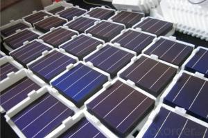
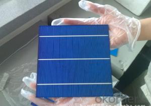
Production:

Package:

FAQ:
1. Q: Do you have your own factory?
A: Yes, we have. Our factory located in Jiangsu
2. Q: How can I visit your factory?
A: Before you visit,please contact us.We will show you the route or arrange a car to pick you up.
3. Q: Do you provide free sample?
A: Commenly we provide paid sample.
4. Q: Could you print our company LOGO on the nameplate and package?
A: Yes, we accept it.And need an Authorization Letter from you.
5. Q: Do you accept custom design on size?
A: Yes, if the size is reasonable.
6. Q: How can I be your agent in my country?
A: Please leave feedback. It's better for us to talk about details by email.
7. Q: Do you have solar project engineer who can guide me to install system?
A: Yes, we have a professional engineer team. They can teach you how to install a solar system.
- Q: How are solar silicon wafers used in solar panels?
- Solar silicon wafers are the key component in solar panels as they act as the building blocks for converting sunlight into electricity. These wafers are made from highly purified silicon and are doped with specific elements to create an electric field. When sunlight hits the wafer, the energy from the photons dislodges electrons, creating a flow of electricity. Multiple wafers are connected together to form a solar cell, and several solar cells are interconnected to construct a solar panel, which can then be used to generate clean and renewable energy.
- Q: What is the role of a bypass diode in a solar silicon wafer?
- The role of a bypass diode in a solar silicon wafer is to prevent power loss caused by shading or partial cell damage. It allows the current to flow around the shaded or damaged area, ensuring a more efficient and uninterrupted flow of electricity from the solar panel.
- Q: How to make resistance on a piece of silicon chip (IC)? Read a lot of related articles, but also the first silicon oxidation, in the end is how? Best draw a
- You say SiO2 is equivalent to the boundary layer and layer.Wiring diagram... Tools are not enough brain.
- Q: Can solar silicon wafers be used in mobile or portable solar chargers?
- Yes, solar silicon wafers can be used in mobile or portable solar chargers. These wafers are commonly used in the production of solar cells, which convert sunlight into electricity. By integrating solar silicon wafers into portable chargers, they can harness solar energy and charge devices on the go.
- Q: What is the purpose of a backsheet in a solar silicon wafer?
- The purpose of a backsheet in a solar silicon wafer is to protect the solar cells from external elements such as moisture, dust, and UV radiation. It acts as a barrier, preventing any damage or degradation to the solar cells, thus ensuring their longevity and optimal performance. Additionally, the backsheet also provides electrical insulation and improves the overall efficiency of the solar panel by reflecting any excess light back onto the solar cells.
- Q: Can solar silicon wafers be used in agricultural irrigation systems?
- No, solar silicon wafers cannot be directly used in agricultural irrigation systems. However, solar panels made from silicon wafers can be used to generate electricity, which can then be used to power water pumps or other components of an agricultural irrigation system.
- Q: Are solar silicon wafers affected by vibrations or shocks?
- Yes, solar silicon wafers can be affected by vibrations or shocks. Excessive vibrations or shocks can cause microcracks, fractures, or dislodgement of the delicate components within the wafer, leading to a decrease in its efficiency or complete failure. It is crucial to handle and transport solar silicon wafers with care to avoid any potential damage.
- Q: What are the different types of solar silicon wafers?
- There are primarily three types of solar silicon wafers: monocrystalline, polycrystalline, and thin-film. Monocrystalline wafers are made from a single crystal structure, offering high efficiency but are more expensive. Polycrystalline wafers are made from multiple crystals, providing lower efficiency but at a lower cost. Thin-film wafers are made from a thin layer of semiconductor material deposited onto a substrate, offering flexibility and lower costs, but with lower efficiency compared to crystalline silicon wafers.
- Q: What is the role of solar silicon wafers in space exploration?
- Solar silicon wafers play a crucial role in space exploration as they are the primary component of solar panels used to generate electricity in space. These wafers are made from highly purified silicon and are capable of converting sunlight into electrical energy, providing a reliable and sustainable power source for space missions. Without solar silicon wafers, it would be challenging to power spacecraft and satellites for long durations in space, limiting our ability to explore and gather valuable data about our universe.
- Q: One hundred watts of solar panels to how many pieces of silicon wafers, 156 of single crystals and polycrystalline
- As for the power, according to the W=UI formula can be obtained, since a single voltage is fixed, the resulting current size determines the power of a battery, the current per tablet produced is not fixed, with the conversion rate of the conversion rate, high current is large, the reverse is small; the same the power conversion rate is high, the area is small
Send your message to us
Solar Silicon Wafer Cassette Compatible High Current 17.2% Polycrystalline Silicon Solar Cell
- Ref Price:
-
- Loading Port:
- Shanghai
- Payment Terms:
- TT OR LC
- Min Order Qty:
- 1000 pc
- Supply Capability:
- 100000 pc/month
OKorder Service Pledge
OKorder Financial Service
Similar products


Hot products


Hot Searches
Related keywords

