


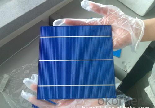

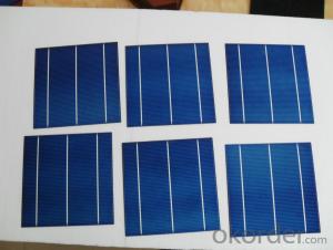
Silicon Wafer Based High Current 17.4% Polycrystalline Silicon Solar Cells
- Ref Price:
-

- Loading Port:
- Shanghai
- Payment Terms:
- TT OR LC
- Min Order Qty:
- 1000 pc
- Supply Capability:
- 100000 pc/month
OKorder Service Pledge
OKorder Financial Service
You Might Also Like


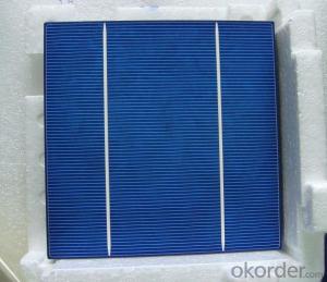
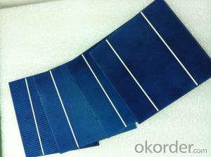
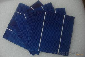
4 Bus Bars 156*156 17.6% efficiency poly solar cell
PHYSICAL CHARACTERISTICS
Dimension: 156mm x 156mm ± 0.5mm
Wafer Thickeness: 180um+20um and 200um+20um
Front(-) Four 1.2mm silver busbar
Silicon nitride blue anti-reflection coating
Back(+) aluminum back surface field
1.75mm(silver) wide segment soldering pads

Typical Electrical Characteristics
Efficiency | W(Pmpp) | V(Umpp) | A(Impp) | V(Uoc) | A(Isc) |
17.4-17.5 | 4.234 | 0.517 | 8.231 | 0.622 | 8.759 |
17.5-17.6 | 4.259 | 0.519 | 8.243 | 0.623 | 8.769 |
17.7-17.8 | 4.283 | 0.521 | 8.256 | 0.625 | 8.779 |
17.8-17.9 | 4.307 | 0.523 | 8.268 | 0.626 | 8.788 |
17.9-18.0 | 4.332 | 0.525 | 8.281 | 0.627 | 8.798 |
18.0-18.1 | 4.380 | 0.529 | 8.306 | 0.629 | 8.808 |
18.1-18.2 | 4.405 | 0.531 | 8.318 | 0.632 | 8.818 |
18.2-18.3 | 4.429 | 0.533 | 8.331 | 0.633 | 8.837 |
18.3-18.4 | 4.453 | 0.535 | 8.344 | 0.634 | 8.847 |
18.4-18.5 | 4.478 | 0.537 | 8.356 | 0.636 | 8.856 |
18.5-18.6 | 4.502 | 0.539 | 8.369 | 0.637 | 8.866 |
Efficiency | W(Pmpp) | V(Umpp) | A(Impp) | V(Uoc) | A(Isc) |
20.90-21.00 | 5.06 | 0.557 | 9.007 | 0.653 | 9.688 |
20.80-20.90 | 5.04 | 0.556 | 9.062 | 0.652 | 9.683 |
20.70-20.80 | 5.02 | 0.554 | 9.055 | 0.651 | 9.684 |
20.60-20.70 | 4.99 | 0.552 | 9.033 | 0.651 | 9.672 |
20.50-20.60 | 4.97 | 0.550 | 9.002 | 0.650 | 9.673 |
20.40-20.50 | 4.94 | 0.548 | 9.012 | 0.649 | 9.674 |
20.30-20.40 | 4.92 | 0.546 | 9.009 | 0.649 | 9.655 |
20.20-20.30 | 4.89 | 0.543 | 9.012 | 0.648 | 9.634 |
20.10-20.20 | 4.87 | 0.541 | 8.998 | 0.648 | 9.617 |
20.00-20.10 | 4.85 | 0.540 | 8.977 | 0.647 | 9.600 |
*Data under standard testing conditional (STC):1,000w/m2,AM1.5, 25°C , Pmax:Positive power tolerance.
3 Bus Bars 156*156 17.4% efficiency poly solar cell
Dimension: 156 mm x 156 mm ± 0.5 mm
Wafer Thickeness: 156 mm x 156 mm ± 0.5 mm

Typical Electrical Characteristics:
| Efficiency code | 1660 | 1680 | 1700 | 1720 | 1740 | 1760 | 1780 | 1800 | 1820 | 1840 | 1860 |
| Efficiency (%) | 16.6 | 16.8 | 17.0 | 17.2 | 17.4 | 17.6 | 17.8 | 18.0 | 18.2 | 18.4 | 18.6 |
| Pmax (W) | 4.04 | 4.09 | 4.14 | 4.19 | 4.23 | 4.28 | 4.33 | 4.38 | 4.43 | 4.48 | 4.53 |
| Voc (V) | 0.612 | 0.615 | 0.618 | 0.621 | 0.624 | 0.627 | 0.629 | 0.63 | 0.633 | 0.635 | 0.637 |
| Isc (A) | 8.42 | 8.46 | 8.51 | 8.56 | 8.61 | 8.65 | 8.69 | 8.73 | 8.77 | 8.81 | 8.84 |
| Imp (A) | 7.91 | 7.99 | 8.08 | 8.16 | 8.22 | 8.27 | 8.33 | 8.38 | 8.43 | 8.48 | 8.53 |
* Testing conditions: 1000 W/m2, AM 1.5, 25 °C, Tolerance: Efficiency ± 0.2% abs., Pmpp ±1.5% rel.
* Imin : at 0.5 V
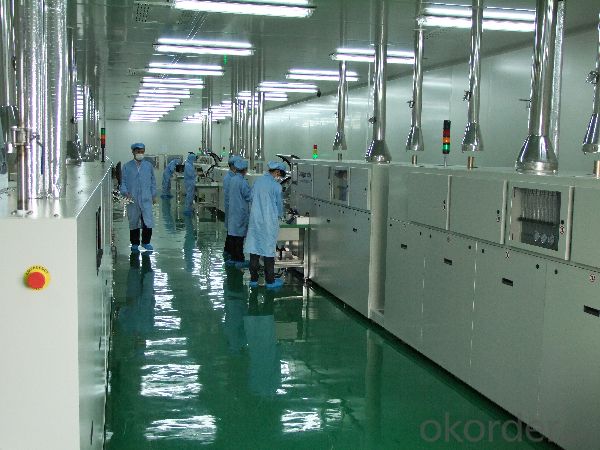
Production:

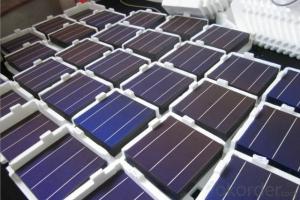
Package:

FAQ:
1. Q: Do you have your own factory?
A: Yes, we have. Our factory located in Jiangsu
2. Q: How can I visit your factory?
A: Before you visit,please contact us.We will show you the route or arrange a car to pick you up.
3. Q: Do you provide free sample?
A: Commenly we provide paid sample.
4. Q: Could you print our company LOGO on the nameplate and package?
A: Yes, we accept it.And need an Authorization Letter from you.
5. Q: Do you accept custom design on size?
A: Yes, if the size is reasonable.
6. Q: How can I be your agent in my country?
A: Please leave feedback. It's better for us to talk about details by email.
7. Q: Do you have solar project engineer who can guide me to install system?
A: Yes, we have a professional engineer team. They can teach you how to install a solar system.
- Q: Can solar silicon wafers be used in solar-powered remote sensing devices?
- Yes, solar silicon wafers can be used in solar-powered remote sensing devices. These wafers are commonly used in photovoltaic cells to convert sunlight into electricity, which can then power various electronic devices, including remote sensing devices. Solar silicon wafers provide a reliable and efficient source of renewable energy for such applications.
- Q: Are solar silicon wafers affected by vibrations?
- Yes, solar silicon wafers can be affected by vibrations. Vibrations can cause microcracks or damage to the delicate structure of the wafer, reducing its efficiency and overall performance. It is important to handle and install solar silicon wafers with care to minimize the risk of damage from vibrations.
- Q: Can solar silicon wafers be used in solar-powered smart cities?
- Yes, solar silicon wafers can be used in solar-powered smart cities. These wafers, which are made from highly purified silicon, are the key component in solar panels that convert sunlight into electricity. By utilizing solar silicon wafers, smart cities can harness renewable energy from the sun to power various infrastructure and devices, reducing reliance on fossil fuels and promoting sustainability.
- Q: Can solar silicon wafers be used in hybrid solar cell technologies?
- Yes, solar silicon wafers can be used in hybrid solar cell technologies. Hybrid solar cells combine different materials to enhance efficiency and expand the range of wavelengths they can convert into electricity. Silicon wafers are commonly used in traditional solar cells, and they can also be integrated into hybrid designs, enabling the incorporation of other materials like perovskites or organic semiconductors. This allows for improved performance and increased versatility in capturing solar energy.
- Q: How are solar silicon wafers protected from electrical faults or short circuits?
- Solar silicon wafers are protected from electrical faults or short circuits through various methods, such as the implementation of anti-reflective coatings, passivation layers, and junction boxes. These protective measures help to prevent direct contact between the conducting materials and the silicon wafer, reducing the likelihood of electrical faults or short circuits. Additionally, quality control measures during the manufacturing process ensure that the wafers are free from any defects or impurities that could potentially lead to electrical issues.
- Q: Can solar silicon wafers be used in thin-film solar cell technology?
- No, solar silicon wafers cannot be used in thin-film solar cell technology. Thin-film solar cells are made using a different manufacturing process and typically use materials such as cadmium telluride or amorphous silicon instead of crystalline silicon wafers.
- Q: How are solar silicon wafers protected from electrical surges?
- Solar silicon wafers are protected from electrical surges through the use of protective devices such as surge suppressors and transient voltage suppressors. These devices are installed in the solar power system to divert excess voltage and current away from the wafers, preventing damage to the delicate electronic components.
- Q: What are the dimensions of a standard solar silicon wafer?
- The standard dimensions of a solar silicon wafer are typically around 156 mm in width and 156 mm in length, with a thickness of about 200-300 micrometers.
- Q: How are solar silicon wafers protected against corrosion?
- Solar silicon wafers are protected against corrosion through the use of passivation techniques. These techniques involve applying a thin layer of protective material, such as silicon nitride or silicon oxide, to the surface of the wafers. This protective layer acts as a barrier, preventing the silicon underneath from coming into contact with moisture or other corrosive elements in the environment. Additionally, the wafers are often encapsulated within a protective module, such as a glass or polymer sheet, which further shields them from corrosion.
- Q: What is the average reflectivity of a solar silicon wafer?
- The average reflectivity of a solar silicon wafer is typically around 30%.
Send your message to us
Silicon Wafer Based High Current 17.4% Polycrystalline Silicon Solar Cells
- Ref Price:
-
- Loading Port:
- Shanghai
- Payment Terms:
- TT OR LC
- Min Order Qty:
- 1000 pc
- Supply Capability:
- 100000 pc/month
OKorder Service Pledge
OKorder Financial Service
Similar products

Hot products


Hot Searches
Related keywords

