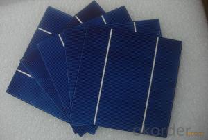


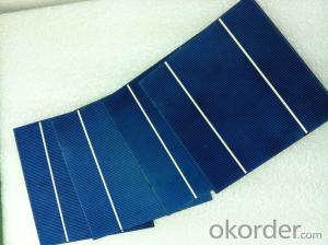
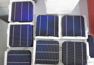
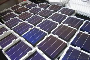
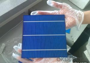
Solar Silicon Wafer Cassette Supplier - High Current 18.0% Polycrystalline Silicon Solar Cell
- Ref Price:
-

- Loading Port:
- Shanghai
- Payment Terms:
- TT OR LC
- Min Order Qty:
- 1000 pc
- Supply Capability:
- 100000 pc/month
OKorder Service Pledge
OKorder Financial Service
You Might Also Like


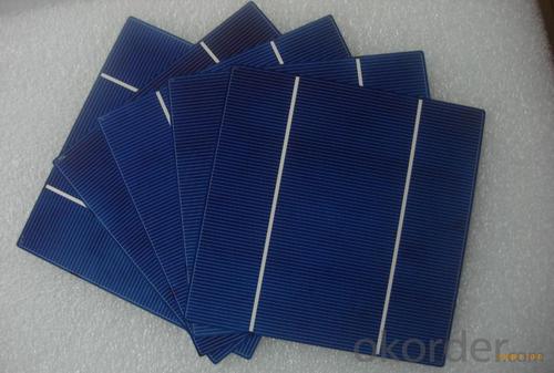
4 Bus Bars 156*156 17.6% efficiency poly solar cell
PHYSICAL CHARACTERISTICS
Dimension: 156mm x 156mm ± 0.5mm
Wafer Thickeness: 180um+20um and 200um+20um
Front(-) Four 1.2mm silver busbar
Silicon nitride blue anti-reflection coating
Back(+) aluminum back surface field
1.75mm(silver) wide segment soldering pads

Typical Electrical Characteristics
Efficiency | W(Pmpp) | V(Umpp) | A(Impp) | V(Uoc) | A(Isc) |
17.4-17.5 | 4.234 | 0.517 | 8.231 | 0.622 | 8.759 |
17.5-17.6 | 4.259 | 0.519 | 8.243 | 0.623 | 8.769 |
17.7-17.8 | 4.283 | 0.521 | 8.256 | 0.625 | 8.779 |
17.8-17.9 | 4.307 | 0.523 | 8.268 | 0.626 | 8.788 |
17.9-18.0 | 4.332 | 0.525 | 8.281 | 0.627 | 8.798 |
18.0-18.1 | 4.380 | 0.529 | 8.306 | 0.629 | 8.808 |
18.1-18.2 | 4.405 | 0.531 | 8.318 | 0.632 | 8.818 |
18.2-18.3 | 4.429 | 0.533 | 8.331 | 0.633 | 8.837 |
18.3-18.4 | 4.453 | 0.535 | 8.344 | 0.634 | 8.847 |
18.4-18.5 | 4.478 | 0.537 | 8.356 | 0.636 | 8.856 |
18.5-18.6 | 4.502 | 0.539 | 8.369 | 0.637 | 8.866 |
Efficiency | W(Pmpp) | V(Umpp) | A(Impp) | V(Uoc) | A(Isc) |
20.90-21.00 | 5.06 | 0.557 | 9.007 | 0.653 | 9.688 |
20.80-20.90 | 5.04 | 0.556 | 9.062 | 0.652 | 9.683 |
20.70-20.80 | 5.02 | 0.554 | 9.055 | 0.651 | 9.684 |
20.60-20.70 | 4.99 | 0.552 | 9.033 | 0.651 | 9.672 |
20.50-20.60 | 4.97 | 0.550 | 9.002 | 0.650 | 9.673 |
20.40-20.50 | 4.94 | 0.548 | 9.012 | 0.649 | 9.674 |
20.30-20.40 | 4.92 | 0.546 | 9.009 | 0.649 | 9.655 |
20.20-20.30 | 4.89 | 0.543 | 9.012 | 0.648 | 9.634 |
20.10-20.20 | 4.87 | 0.541 | 8.998 | 0.648 | 9.617 |
20.00-20.10 | 4.85 | 0.540 | 8.977 | 0.647 | 9.600 |
*Data under standard testing conditional (STC):1,000w/m2,AM1.5, 25°C , Pmax:Positive power tolerance.
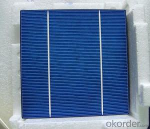
3 Bus Bars 156*156 17.4% efficiency poly solar cell
Dimension: 156 mm x 156 mm ± 0.5 mm
Wafer Thickeness: 156 mm x 156 mm ± 0.5 mm

Typical Electrical Characteristics:
| Efficiency code | 1660 | 1680 | 1700 | 1720 | 1740 | 1760 | 1780 | 1800 | 1820 | 1840 | 1860 |
| Efficiency (%) | 16.6 | 16.8 | 17.0 | 17.2 | 17.4 | 17.6 | 17.8 | 18.0 | 18.2 | 18.4 | 18.6 |
| Pmax (W) | 4.04 | 4.09 | 4.14 | 4.19 | 4.23 | 4.28 | 4.33 | 4.38 | 4.43 | 4.48 | 4.53 |
| Voc (V) | 0.612 | 0.615 | 0.618 | 0.621 | 0.624 | 0.627 | 0.629 | 0.63 | 0.633 | 0.635 | 0.637 |
| Isc (A) | 8.42 | 8.46 | 8.51 | 8.56 | 8.61 | 8.65 | 8.69 | 8.73 | 8.77 | 8.81 | 8.84 |
| Imp (A) | 7.91 | 7.99 | 8.08 | 8.16 | 8.22 | 8.27 | 8.33 | 8.38 | 8.43 | 8.48 | 8.53 |
* Testing conditions: 1000 W/m2, AM 1.5, 25 °C, Tolerance: Efficiency ± 0.2% abs., Pmpp ±1.5% rel.
* Imin : at 0.5 V
Production:

Package:

FAQ:
1. Q: Do you have your own factory?
A: Yes, we have. Our factory located in Jiangsu
2. Q: How can I visit your factory?
A: Before you visit,please contact us.We will show you the route or arrange a car to pick you up.
3. Q: Do you provide free sample?
A: Commenly we provide paid sample.
4. Q: Could you print our company LOGO on the nameplate and package?
A: Yes, we accept it.And need an Authorization Letter from you.
5. Q: Do you accept custom design on size?
A: Yes, if the size is reasonable.
6. Q: How can I be your agent in my country?
A: Please leave feedback. It's better for us to talk about details by email.
7. Q: Do you have solar project engineer who can guide me to install system?
A: Yes, we have a professional engineer team. They can teach you how to install a solar system.
- Q: How do solar silicon wafers contribute to reducing carbon emissions?
- Solar silicon wafers contribute to reducing carbon emissions by enabling the production of solar panels, which generate clean and renewable electricity from sunlight. As the main component of solar cells, silicon wafers capture sunlight and convert it into electrical energy without emitting greenhouse gases or pollutants. By replacing fossil fuel-based energy sources, solar silicon wafers help reduce reliance on carbon-intensive electricity generation, ultimately mitigating carbon emissions and combating climate change.
- Q: What is the role of solar silicon wafers in reducing water consumption?
- Solar silicon wafers play a crucial role in reducing water consumption in the production of solar panels. Unlike traditional energy sources, solar energy generation does not require water for its operation. By generating electricity from sunlight using solar silicon wafers, we can significantly reduce the need for water-intensive energy generation methods such as coal or natural gas power plants. This helps conserve water resources, minimize water pollution, and promote a more sustainable and environmentally friendly energy production system.
- Q: The process for steel wire cutting silicon factory, we use HCTB5 wire, you can do?
- Mortar free multi wire cuttingMortar free type multi wire cutting, cutting and cutting sand coexist in the grinding fluid, resulting in low cutting efficiency; and the high viscosity of the coolant and cutting sand and high value of cutting raw materials mixed together, separation is difficult, resulting in the waste of raw materials and environmental pollution.Diamond wire cuttingThe preparation technology of diamond wire belongs to the technology of consolidation abrasive particles. Fixed abrasive wire cutting way between the consolidation in the wire on the abrasive and workpiece material cutting based on the principle of two body wear, abrasive particles directly on the workpiece, which belongs to a kind of rigid cutting method, greatly improves the cutting efficiency.
- Q: How are solar silicon wafers connected to form a solar cell?
- Solar silicon wafers are connected to form a solar cell through a process called cell interconnection. This involves soldering or gluing thin metal strips, usually made of silver, on the front and back surfaces of the wafers. These metal strips, known as busbars, act as conductive pathways, connecting the positive and negative sides of the individual silicon wafers. By linking multiple wafers together in this manner, they are able to generate a higher voltage and current, resulting in a more efficient solar cell.
- Q: What is the purpose of a tracker in a solar silicon wafer?
- The purpose of a tracker in a solar silicon wafer is to maximize the efficiency of solar energy generation by orienting the wafer towards the sun, ensuring optimal exposure to sunlight throughout the day.
- Q: How to calculate the conversion efficiency of monocrystalline silicon
- Proportion of dark current - Irev>6 cell ratioThe proportion of low efficiency tablets - the proportion of P156Eff<14.5% batteries8 inch single crystal conversion rate of about 18.5%; a single conversion rate of about 9 inches in about 18.6%; quasi single crystal (large particles) probably about 18%; the new diamond wire cutting rate can be converted to about 18.92%.
- Q: How are solar silicon wafers protected from theft?
- Solar silicon wafers are typically protected from theft through various security measures. These may include surveillance cameras, alarm systems, secure storage facilities, and restricted access to the production areas. Additionally, tracking technologies like RFID tags or GPS can be used to monitor and locate stolen wafers. These measures aim to deter theft, detect any unauthorized activity, and enable quick recovery in case of theft.
- Q: How do solar silicon wafers perform in urban environments?
- Solar silicon wafers generally perform well in urban environments. However, their efficiency may be slightly affected by factors like shading from nearby buildings or pollution in the air. Despite these challenges, advancements in solar technology and installation techniques have made it possible to maximize solar energy generation in urban areas.
- Q: What's the difference between a silicon wafer and a battery?
- Silicon wafers are cut into pieces by wire cutting!The battery pack is a silicon wafer through the surface flocking, diffusion of PN junction, and then PECVD coating
- Q: How to extract silicon from silicon wafers
- Slice: cut a single crystal silicon rod into a thin wafer with an exact geometry. In this process, the silica fume is produced by water leaching to produce waste water and silicon slag.
Send your message to us
Solar Silicon Wafer Cassette Supplier - High Current 18.0% Polycrystalline Silicon Solar Cell
- Ref Price:
-
- Loading Port:
- Shanghai
- Payment Terms:
- TT OR LC
- Min Order Qty:
- 1000 pc
- Supply Capability:
- 100000 pc/month
OKorder Service Pledge
OKorder Financial Service
Similar products

Hot products


Hot Searches
Related keywords

