


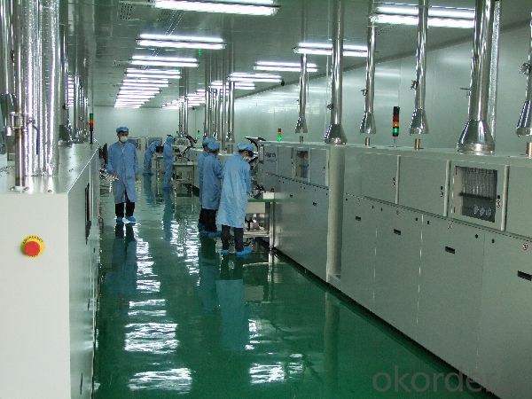

China Solar Silicon Wafer Cassette - High Quality A Grade Polycrystalline Solar Cell 5V 15.8%
- Ref Price:
-

- Loading Port:
- Shanghai
- Payment Terms:
- TT OR LC
- Min Order Qty:
- 1000 pc
- Supply Capability:
- 100000 pc/month
OKorder Service Pledge
OKorder Financial Service
You Might Also Like


Specifications
hot sale solar cell
1.16.8%~18.25% high efficiency
2.100% checked quality
3.ISO9001/ISO14001/TUV/CE/UL
4.stable performance
We can offer you the best quality products and services, don't miss !
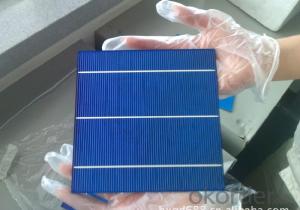
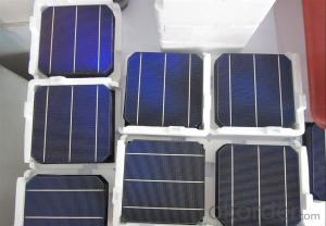
POLY6'(156*156)
Polycrystalline Silicon Solar cell
Physical Characteristics
Dimension: 156mm×156mm±0.5mm
Diagonal: 220mm±0.5mm
Thickness(Si): 200±20 μm
Front(-) Back(+)
Blue anti-reflecting coating (silicon nitride); Aluminum back surface field;
1.5mm wide bus bars; 2.0mm wide soldering pads;
Distance between bus bars: 51mm . Distance between bus bars :51mm .
Electrical Characteristics
Efficiency(%) | 18.00 | 17.80 | 17.60 | 17.40 | 17.20 | 16.80 | 16.60 | 16.40 | 16.20 | 16.00 | 15.80 | 15.60 |
Pmpp(W) | 4.33 | 4.29 | 4.24 | 4.19 | 4.14 | 4.09 | 4.04 | 3.99 | 3.94 | 3.90 | 3.86 | 3.82 |
Umpp(V) | 0.530 | 0.527 | 0.524 | 0.521 | 0.518 | 0.516 | 0.514 | 0.511 | 0.509 | 0.506 | 0.503 | 0.501 |
Impp(A) | 8.159 | 8.126 | 8.081 | 8.035 | 7.990 | 7.938 | 7.876 | 7.813 | 7.754 | 7.698 | 7.642 | 7.586 |
Uoc(V) | 0.633 | 0.631 | 0.628 | 0.625 | 0.623 | 0.620 | 0.618 | 0.617 | 0.615 | 0.613 | 0.611 | 0.609 |
Isc(A) | 8.709 | 8.677 | 8.629 | 8.578 | 8.531 | 8.478 | 8.419 | 8.356 | 8.289 | 8.220 | 8.151 | 8.083 |

MONO5'(125*125mm)165
Monocrystalline silicon solar cell
Physical Characteristics
Dimension: 125mm×125mm±0.5mm
Diagonal: 165mm±0.5mm
Thickness(Si): 200±20 μm
Front(-) Back(+)
Blue anti-reflecting coating(silicon nitride); Aluminum back surface field;
1.6mmwide bus bars; 2.5mm wide soldering pads;
Distance between bus bars: 61mm . Distance between bus bars :61mm .
Electrical Characteristics
Efficiency(%) | 19.40 | 19.20 | 19.00 | 18.80 | 18.60 | 18.40 | 18.20 | 18.00 | 17.80 | 17.60 | 17.40 | 17.20 |
Pmpp(W) | 2.97 | 2.94 | 2.91 | 2.88 | 2.85 | 2.82 | 2.79 | 2.76 | 2.73 | 2.70 | 2.67 | 2.62 |
Umpp(V) | 0.537 | 0.535 | 0.533 | 0.531 | 0.527 | 0.524 | 0.521 | 0.518 | 0.516 | 0.515 | 0.513 | 0.509 |
Impp(A) | 5.531 | 5.495 | 5.460 | 5.424 | 5.408 | 5.382 | 5.355 | 5.328 | 5.291 | 5.243 | 5.195 | 4.147 |
Uoc(V) | 0.637 | 0.637 | 0.636 | 0.635 | 0.633 | 0.630 | 0.629 | 0.629 | 0.628 | 0.626 | 0.626 | 0.625 |
Isc(A) | 5.888 | 5.876 | 5.862 | 5.848 | 5.839 | 5.826 | 5.809 | 5.791 | 5.779 | 5.756 | 5.293 | 5.144 |

FAQ:
Q:How can i get some sample?
A:Yes , if you want order ,sample is not a problem.
Q:How about your solar panel efficency?
A: Our product efficency around 17.25%~18.25%.
Q:What’s the certificate you have got?
A: we have overall product certificate of ISO9001/ISO14001/CE/TUV/UL
- Q: What is the effect of spectral response on the efficiency of a solar silicon wafer?
- The spectral response refers to how well a solar silicon wafer converts different wavelengths of light into electricity. A high spectral response means that the wafer can efficiently convert a wide range of wavelengths, resulting in higher overall efficiency. Conversely, a low spectral response means that the wafer may not be able to convert certain wavelengths effectively, leading to reduced efficiency. Therefore, the spectral response plays a crucial role in determining the efficiency of a solar silicon wafer.
- Q: What are the different types of junction box sealants used on solar silicon wafers?
- There are several types of junction box sealants used on solar silicon wafers, including silicone, epoxy, and polyurethane. These sealants are applied to protect the junction box and its components from moisture, dust, and other environmental factors, ensuring the long-term durability and performance of the solar panels.
- Q: Can solar silicon wafers be used in electric vehicle charging stations?
- Yes, solar silicon wafers can be used in electric vehicle charging stations. They can be utilized to capture sunlight and convert it into electricity, which can then be used to power the charging stations, providing a sustainable and renewable source of energy for electric vehicles.
- Q: 8 inch monocrystalline silicon area?
- 8 inches =20.32cm8 inch monocrystalline silicon area of =Pi*10.16*10.16=324.29 square centimeters
- Q: How much is the thickness of the silicon wafer
- For integrated circuits: generally 4 inch wafer thickness of 0.520mm, the thickness of the 6 inch wafer
- Q: How do solar silicon wafers perform in dusty or sandy environments?
- Solar silicon wafers can be affected by dust or sand particles in the environment. When the surface of the wafers gets covered with dust or sand, it can reduce the amount of sunlight reaching the solar cells, thereby decreasing their efficiency. Additionally, the accumulation of dust or sand can create hotspots and increase the temperature of the wafers, which can further impact their performance. Therefore, it is important to regularly clean and maintain solar silicon wafers in dusty or sandy environments to ensure optimal efficiency and longevity.
- Q: How are solar silicon wafers connected in a solar array?
- Solar silicon wafers are typically connected in a solar array through a process called soldering. Soldering involves joining the wafers together using a conductive material, such as silver paste or copper ribbon, which creates electrical connections between the individual cells. This allows the solar cells to work collectively and generate electricity when exposed to sunlight.
- Q: How do solar silicon wafers perform in earthquake-prone environments?
- Solar silicon wafers perform well in earthquake-prone environments due to their inherent durability and flexibility. The rigid structure of the wafers allows them to withstand seismic activities without significant damage or loss of functionality. Additionally, advancements in solar panel mounting systems have further enhanced their resilience by incorporating features such as shock-absorbing mechanisms and reinforced support structures. Overall, solar silicon wafers have proven to be reliable and robust in earthquake-prone areas, ensuring the continuous generation of clean energy.
- Q: How is a junction box sealant applied to a solar silicon wafer?
- A junction box sealant is typically applied to a solar silicon wafer by using a precise application technique. The sealant is carefully dispensed onto the junction box area of the wafer, ensuring complete coverage and a secure seal. This helps protect the components inside the junction box from environmental factors and ensures the long-term performance of the solar panel.
- Q: Are solar silicon wafers affected by snow or ice accumulation?
- Yes, solar silicon wafers can be affected by snow or ice accumulation. Snow or ice covering the solar panels can reduce their efficiency by blocking sunlight from reaching the silicon wafers, which are responsible for converting solar energy into electricity. Additionally, the weight of accumulated snow or ice can put stress on the panels and potentially cause damage if they are not designed to withstand such loads. Regular cleaning or installing tilt systems can help mitigate the impact of snow or ice accumulation on solar silicon wafers.
Send your message to us
China Solar Silicon Wafer Cassette - High Quality A Grade Polycrystalline Solar Cell 5V 15.8%
- Ref Price:
-
- Loading Port:
- Shanghai
- Payment Terms:
- TT OR LC
- Min Order Qty:
- 1000 pc
- Supply Capability:
- 100000 pc/month
OKorder Service Pledge
OKorder Financial Service
Similar products


Hot products


Hot Searches
Related keywords

