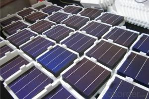


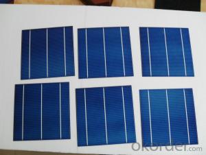
Solar Panel Silicon Wafer - High Current 16.6% Polycrystalline Silicon Solar Cell
- Ref Price:
-

- Loading Port:
- Shanghai
- Payment Terms:
- TT OR LC
- Min Order Qty:
- 1000 pc
- Supply Capability:
- 100000 pc/month
OKorder Service Pledge
OKorder Financial Service
You Might Also Like


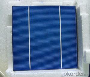
4 Bus Bars 156*156 17.6% efficiency poly solar cell
PHYSICAL CHARACTERISTICS
Dimension: 156mm x 156mm ± 0.5mm
Wafer Thickeness: 180um+20um and 200um+20um
Front(-) Four 1.2mm silver busbar
Silicon nitride blue anti-reflection coating
Back(+) aluminum back surface field
1.75mm(silver) wide segment soldering pads

Typical Electrical Characteristics
Efficiency | W(Pmpp) | V(Umpp) | A(Impp) | V(Uoc) | A(Isc) |
17.4-17.5 | 4.234 | 0.517 | 8.231 | 0.622 | 8.759 |
17.5-17.6 | 4.259 | 0.519 | 8.243 | 0.623 | 8.769 |
17.7-17.8 | 4.283 | 0.521 | 8.256 | 0.625 | 8.779 |
17.8-17.9 | 4.307 | 0.523 | 8.268 | 0.626 | 8.788 |
17.9-18.0 | 4.332 | 0.525 | 8.281 | 0.627 | 8.798 |
18.0-18.1 | 4.380 | 0.529 | 8.306 | 0.629 | 8.808 |
18.1-18.2 | 4.405 | 0.531 | 8.318 | 0.632 | 8.818 |
18.2-18.3 | 4.429 | 0.533 | 8.331 | 0.633 | 8.837 |
18.3-18.4 | 4.453 | 0.535 | 8.344 | 0.634 | 8.847 |
18.4-18.5 | 4.478 | 0.537 | 8.356 | 0.636 | 8.856 |
18.5-18.6 | 4.502 | 0.539 | 8.369 | 0.637 | 8.866 |
Efficiency | W(Pmpp) | V(Umpp) | A(Impp) | V(Uoc) | A(Isc) |
20.90-21.00 | 5.06 | 0.557 | 9.007 | 0.653 | 9.688 |
20.80-20.90 | 5.04 | 0.556 | 9.062 | 0.652 | 9.683 |
20.70-20.80 | 5.02 | 0.554 | 9.055 | 0.651 | 9.684 |
20.60-20.70 | 4.99 | 0.552 | 9.033 | 0.651 | 9.672 |
20.50-20.60 | 4.97 | 0.550 | 9.002 | 0.650 | 9.673 |
20.40-20.50 | 4.94 | 0.548 | 9.012 | 0.649 | 9.674 |
20.30-20.40 | 4.92 | 0.546 | 9.009 | 0.649 | 9.655 |
20.20-20.30 | 4.89 | 0.543 | 9.012 | 0.648 | 9.634 |
20.10-20.20 | 4.87 | 0.541 | 8.998 | 0.648 | 9.617 |
20.00-20.10 | 4.85 | 0.540 | 8.977 | 0.647 | 9.600 |
*Data under standard testing conditional (STC):1,000w/m2,AM1.5, 25°C , Pmax:Positive power tolerance.
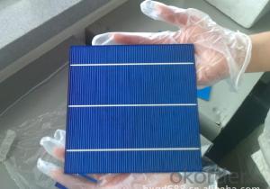
3 Bus Bars 156*156 17.4% efficiency poly solar cell
Dimension: 156 mm x 156 mm ± 0.5 mm
Wafer Thickeness: 156 mm x 156 mm ± 0.5 mm

Typical Electrical Characteristics:
| Efficiency code | 1660 | 1680 | 1700 | 1720 | 1740 | 1760 | 1780 | 1800 | 1820 | 1840 | 1860 |
| Efficiency (%) | 16.6 | 16.8 | 17.0 | 17.2 | 17.4 | 17.6 | 17.8 | 18.0 | 18.2 | 18.4 | 18.6 |
| Pmax (W) | 4.04 | 4.09 | 4.14 | 4.19 | 4.23 | 4.28 | 4.33 | 4.38 | 4.43 | 4.48 | 4.53 |
| Voc (V) | 0.612 | 0.615 | 0.618 | 0.621 | 0.624 | 0.627 | 0.629 | 0.63 | 0.633 | 0.635 | 0.637 |
| Isc (A) | 8.42 | 8.46 | 8.51 | 8.56 | 8.61 | 8.65 | 8.69 | 8.73 | 8.77 | 8.81 | 8.84 |
| Imp (A) | 7.91 | 7.99 | 8.08 | 8.16 | 8.22 | 8.27 | 8.33 | 8.38 | 8.43 | 8.48 | 8.53 |
* Testing conditions: 1000 W/m2, AM 1.5, 25 °C, Tolerance: Efficiency ± 0.2% abs., Pmpp ±1.5% rel.
* Imin : at 0.5 V
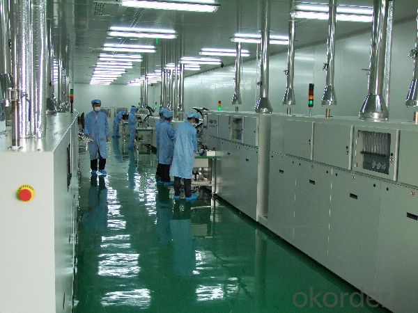
Production:

Package:

FAQ:
1. Q: Do you have your own factory?
A: Yes, we have. Our factory located in Jiangsu
2. Q: How can I visit your factory?
A: Before you visit,please contact us.We will show you the route or arrange a car to pick you up.
3. Q: Do you provide free sample?
A: Commenly we provide paid sample.
4. Q: Could you print our company LOGO on the nameplate and package?
A: Yes, we accept it.And need an Authorization Letter from you.
5. Q: Do you accept custom design on size?
A: Yes, if the size is reasonable.
6. Q: How can I be your agent in my country?
A: Please leave feedback. It's better for us to talk about details by email.
7. Q: Do you have solar project engineer who can guide me to install system?
A: Yes, we have a professional engineer team. They can teach you how to install a solar system.
- Q: Are solar silicon wafers affected by electromagnetic interference (EMI)?
- Yes, solar silicon wafers can be affected by electromagnetic interference (EMI). EMI refers to the disruption caused by electromagnetic fields on electronic devices, and solar silicon wafers, being electronic components used in solar panels, are not immune to this interference. EMI can potentially impact the efficiency and performance of solar panels, leading to a decrease in power output. Therefore, it is important to consider EMI mitigation techniques during the design and installation of solar systems to minimize its impact on the silicon wafers and overall solar panel performance.
- Q: How do solar silicon wafers perform in dusty and sandy environments?
- Solar silicon wafers tend to perform less efficiently in dusty and sandy environments. The accumulation of dust and sand particles on the surface of the wafers can block sunlight and reduce the amount of light absorbed by the solar cells. This can result in a decrease in the overall energy production of the solar panels. Regular cleaning and maintenance are necessary to ensure optimal performance in such environments.
- Q: Are solar silicon wafers affected by ultraviolet (UV) radiation?
- Yes, solar silicon wafers are affected by ultraviolet (UV) radiation. UV radiation can cause degradation and damage to the silicon material used in solar cells, reducing their efficiency and overall performance over time. Therefore, it is important to take precautions and use protective coatings or materials to minimize the impact of UV radiation on solar silicon wafers.
- Q: What is the global production capacity of solar silicon wafers?
- The global production capacity of solar silicon wafers is difficult to determine as it varies over time due to market demand and production expansions. However, as of 2021, it is estimated to be in the range of several tens of gigawatts per year.
- Q: Can solar silicon wafers be used in solar-powered educational institutions?
- Yes, solar silicon wafers can be used in solar-powered educational institutions. These wafers are a crucial component of solar panels, which generate electricity from sunlight. Solar-powered educational institutions can install solar panels using silicon wafers to harness renewable energy and reduce dependence on traditional power sources. This sustainable energy solution can help these institutions become more environmentally friendly while educating students about the benefits of solar power.
- Q: Can solar silicon wafers be used in solar-powered wearable devices?
- Yes, solar silicon wafers can be used in solar-powered wearable devices. These wafers are commonly used in solar panels and can be adapted for use in smaller, portable devices such as wearables. By integrating solar silicon wafers into the design of wearable devices, they can harness solar energy to power various functions or even charge the device's battery. This enables wearables to become more self-sustaining and reduce the reliance on traditional charging methods.
- Q: How are solar silicon wafers affected by dust or dirt accumulation?
- Solar silicon wafers are negatively affected by dust or dirt accumulation as they can reduce the efficiency of the solar cells. The accumulation of dust or dirt on the surface of the wafers creates a barrier that prevents sunlight from reaching the solar cells, resulting in reduced energy production. Regular cleaning and maintenance are crucial to ensure optimal performance of solar panels.
- Q: How are solar silicon wafers affected by photon recycling?
- Solar silicon wafers are positively affected by photon recycling as it allows for more efficient use of photons. When photons are not absorbed by the first pass through the wafer, they have a chance to be reflected back and have another opportunity to be absorbed. This recycling process increases the overall absorption of photons, resulting in improved energy conversion efficiency of solar cells.
- Q: Silicon wafer is not light mixed with heavy doping?That is not mixed with P type N type, then ask what is the meaning of SUBThere are light doped tablets with heavy doping in the semiconductor industry is how to express?
- Otherwise, the light is mixed, N++/P++ said heavy doping, no plus is light, thank you
- Q: What is the expected degradation rate of a solar silicon wafer over time?
- The expected degradation rate of a solar silicon wafer over time can vary depending on various factors such as the quality of the wafer, the manufacturing process, and the environmental conditions it is exposed to. However, on average, a well-maintained silicon wafer can experience a degradation rate of around 0.5% to 1% per year.
Send your message to us
Solar Panel Silicon Wafer - High Current 16.6% Polycrystalline Silicon Solar Cell
- Ref Price:
-
- Loading Port:
- Shanghai
- Payment Terms:
- TT OR LC
- Min Order Qty:
- 1000 pc
- Supply Capability:
- 100000 pc/month
OKorder Service Pledge
OKorder Financial Service
Similar products


Hot products


Hot Searches
Related keywords

