
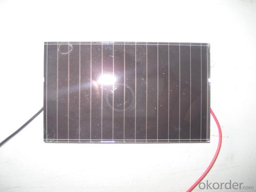
Solar Grade Silicon Wafer Amorphous Silicon Dice Specification 6
- Ref Price:
-

- Loading Port:
- China Main Port
- Payment Terms:
- TT OR LC
- Min Order Qty:
- -
- Supply Capability:
- -
OKorder Service Pledge
OKorder Financial Service
You Might Also Like


Pv modules at present, the mainstream products are still in silicon as the main raw materials, only in terms of silicon raw material consumption, production 1 mw of crystalline silicon solar cell, need 10 to 12 tons of high purity silicon, but if use the same silicon materials used to produce thin film amorphous silicon solar cell can produce more than 200 mw.
From the perspective of energy consumption, amorphous silicon solar battery only 1-1.5 years of energy recovery period, more embodies its contribution to energy saving in the manufacturing process.
Component occupies a high proportion of costs in a photovoltaic system, the component prices directly affect the system cost, and thus affect the cost of photovoltaic power generation. Calculated at the current price of components, the same money, buy amorphous silicon products, you can get more close to 30% of the power components.
2, more power
For the same power of solar cell array, amorphous silicon solar cell is about 10% more than monocrystalline silicon, polycrystalline silicon battery power. This has been the Uni - Solar System LLC, Energy Photovoltaic Corp., Japan's Kaneka Corp., the Netherlands Energy research institute, and other organizations and experts confirmed that the Photovoltaic industry.
In sunny, that is to say, under the high temperature, amorphous silicon solar cell components can show more excellent power performance.
3, better low light response
Due to the characteristics of amorphous silicon atoms are arranged disorderly, the electron transition no longer comply with the restriction of traditional \"selection rule\", as a result, its light absorption characteristics and there are big differences monocrystalline silicon material. Amorphous silicon and monocrystalline silicon material absorption curve as shown
, amorphous silicon absorption curve has obvious three sections (A, B, C). Area A corresponding electronic transition between localized states, such as the gap state near Fermi level and to the tail state transition, the absorption coefficient is small, about 1-10 cm - 1, for this is absorbing; B area absorption coefficient with the increase of the photon energy index rose, it corresponds to the electrons from the valence band edge extension state to the conduction band localized state transition, as well as the localized electrons from the valence band tail states guide for edge extension state transition, the region's energy range is usually only about half of the electron volts, but absorption coefficient across two or three orders of magnitude, usually up to 104 cm - 1; Area C corresponds to the electrons from the valence band to the conduction band internal internal transition, the absorption coefficient is bigger, often in more than 104 cm - 1. After two absorption area is crystalline silicon eigen absorption area.
Can be seen in the figure, the intersection of two curves about 1.8 ev. It is important to note that in the visible light range (1.7 to 3.0 ev), the absorption coefficient of amorphous silicon material is almost an order of magnitude larger than the single crystal silicon. That is to say, in the morning the first part of the sun is not too strong, the second half, and it's cloudy in the afternoon under the condition of low light intensity, long wave is greater, the amorphous silicon material still has a large absorption coefficient. Again considering the amorphous silicon band gap is larger, the reverse saturation current I0 is smaller. And as mentioned the amorphous silicon battery the characteristics I - V characteristic curve of the amorphous silicon solar cell both in theory and in practical use in low light intensity has good adaptation.
• I - V characteristics of amorphous silicon cells after more than a Vm with the voltage drop slowly
In order to be convenient, we draw the I - V characteristics of two kinds of batteries on the same picture. Crystalline silicon and amorphous silicon battery I - V characteristics of general shape as shown
we see from the picture, two kinds of cells in the curve changes after exceed the maximum output power point gap is bigger. Output current of crystalline silicon cells after exceed the maximum output power point will soon fall to zero, curve steep; Rather than crystalline silicon cells output current after a long distance to fall to zero, the curve is relatively flat. Two kinds of battery Vm equivalent to about 83% of its open circuit voltage and 83% respectively.
when light intensity gradually become hour, short circuit current and open circuit voltage of solar battery will be stronger. Short circuit current decreases faster, of course, open circuit voltage decrease more slowly.
do in battery solar cell array under the condition of load, when the sun battery array of effective output voltage less than the terminal voltage of battery, battery cannot be recharged. When the light intensity gradually become hour, crystal silicon battery charging does not meet the conditions, and amorphous silicon due to the larger voltage difference, do not charge until the light is very dark, effectively increase the use of sunlight time. So, amorphous silicon cells to produce more electricity than the crystalline silicon.
4, more excellent high temperature performance
High in the outdoor environment temperature, amorphous silicon solar cell performance change, depends on the temperature, spectrum, as well as other related factors. But what is certain is: amorphous silicon than monocrystalline silicon or polycrystalline silicon are less likely to be affected by temperature.
Amorphous silicon solar cells than monocrystalline silicon, polycrystalline silicon cells have relatively small temperature coefficient of amorphous silicon solar cell output power best Pm temperature coefficient is about 0.19%, and monocrystalline silicon, polycrystalline silicon cells best output power Pm temperature coefficient is about 0.5%, when the battery work at higher temperatures, the two batteries will be a drop in the Pm, but the decline is different. They can be calculated using the following formula.
- Q: What is the cost of manufacturing a solar silicon wafer?
- The cost of manufacturing a solar silicon wafer can vary depending on various factors such as the size, quality, and quantity required. On average, the cost can range from a few cents to a few dollars per wafer.
- Q: What is the purpose of a microinverter in a solar silicon wafer?
- The purpose of a microinverter in a solar silicon wafer is to convert the direct current (DC) generated by the solar panel into alternating current (AC) that can be used to power electrical devices or fed back into the grid. It ensures that each individual solar panel operates at its maximum efficiency and allows for better monitoring and control of the overall solar power system.
- Q: How are solar silicon wafers protected from oxidation?
- Solar silicon wafers are protected from oxidation by applying a thin layer of passivation material, such as silicon nitride or silicon dioxide, on their surface. This layer acts as a protective barrier, preventing oxygen from reaching the silicon and thus inhibiting the oxidation process.
- Q: How is a junction box integrated into a solar silicon wafer?
- A junction box is typically integrated into a solar silicon wafer by being attached to the backside of the wafer. The junction box houses the electrical connections and components necessary for the solar panel to function, such as diodes, bypass diodes, and connectors. It is securely sealed to protect the components from environmental factors and ensure reliable performance.
- Q: What is the typical doping material used in solar silicon wafers?
- The typical doping material used in solar silicon wafers is usually boron for p-type doping and phosphorus for n-type doping.
- Q: Can solar silicon wafers be used in hybrid solar energy systems?
- Yes, solar silicon wafers can indeed be used in hybrid solar energy systems. Hybrid solar energy systems combine different technologies, such as photovoltaic (PV) solar panels and concentrated solar power (CSP) systems, to maximize energy generation. Silicon wafers are commonly used in PV solar panels, which convert sunlight directly into electricity. Therefore, incorporating silicon wafers into hybrid solar energy systems can effectively contribute to the overall energy production of the system.
- Q: I grew up in the silicon chip Ag particles, the size of about a few hundred nanometers, I would like to ask how I do before the TEM sample?
- And then use the copper net fishing, so that particles attached to the copper network.
- Q: How does the efficiency of a solar silicon wafer change with time of day?
- The efficiency of a solar silicon wafer typically fluctuates with the time of day. It tends to be highest during peak sunlight hours, which are typically around midday, and decreases as the sun moves closer to sunrise or sunset. This is because the intensity of sunlight is strongest when the sun is directly overhead, providing maximum energy for the solar panel to convert into electricity. As the angle of the sun changes throughout the day, the amount of sunlight reaching the solar wafer reduces, resulting in a decrease in efficiency.
- Q: How do solar silicon wafers perform in high-altitude environments?
- Solar silicon wafers perform well in high-altitude environments. The thin layer of silicon on the wafers allows for efficient absorption of sunlight, even at higher altitudes where the air is thinner. Additionally, solar panels are designed to withstand various environmental conditions, including temperature changes and exposure to UV radiation. Therefore, solar silicon wafers are suitable for generating electricity in high-altitude areas.
- Q: What is the effect of impurities on the performance of solar silicon wafers?
- The presence of impurities in solar silicon wafers can have a significant effect on their performance. Impurities can alter the electrical conductivity and optical properties of the wafers, leading to decreased efficiency in converting sunlight into electricity. They can also introduce defects, such as dislocations and stacking faults, which can reduce the durability and reliability of the wafers. Therefore, minimizing impurities is crucial in ensuring optimal performance and longevity of solar silicon wafers.
Send your message to us
Solar Grade Silicon Wafer Amorphous Silicon Dice Specification 6
- Ref Price:
-
- Loading Port:
- China Main Port
- Payment Terms:
- TT OR LC
- Min Order Qty:
- -
- Supply Capability:
- -
OKorder Service Pledge
OKorder Financial Service
Similar products


Hot products


Hot Searches
Related keywords

