
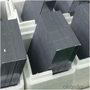


Silicon Wafer Solar Cell - 4w S Grade 156.75*156.75mm Polycrystalline Solar Cell
- Ref Price:
-

- Loading Port:
- China main port
- Payment Terms:
- TT or LC
- Min Order Qty:
- 100 watt
- Supply Capability:
- 10000 watt/month
OKorder Service Pledge
OKorder Financial Service
You Might Also Like


4W A Grade 156.75*156.75mm Polycrystalline Solar Cell
Solar Module Summarize
Solar Module is the core part of solar PV power systems,also is the highest value part of it. The function of Solor Module is to convert the sun's radiation to electrical energy, or transfer it to battery and store in it, or to drive the load running.
The Product has been widely used in space and ground, it mainly used for power generation systems, charging systems, road lighting and traffic signs areas. It could offer a wide range of power and voltage, and with high conversion efficiency, and long service life.
Main Characteristic
Long Service Life
High Efficiency Solar Cells
Special Aluminum Frame Design
High Transmission, Low Iron Tempered Glass
Advanced Cell Encapsulation
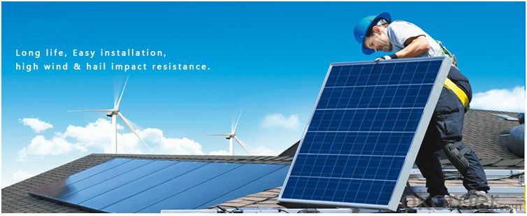
APPLICATIONS
Solar power stations
Rural electrification, Small home power systems
Power supply for traffic, security, gas industry
12V and 24V battery charging system
Other industrial and commercial application
Typical I-V curve

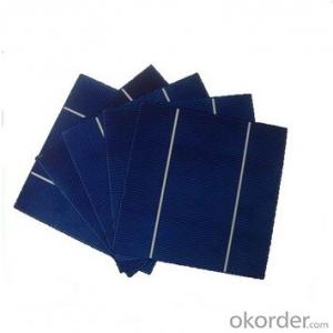
Product Show


Warranties
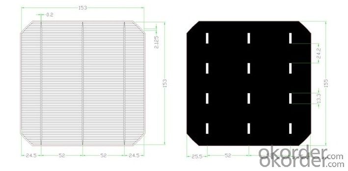
6Inch 2BB Polycrystalline Multi Solar Cells Mono Solar Cell
For c-Si panel: 25years output warranty for no less than 80% of performance, 10 years output warranty for no less than 90% of performance. Free from material and workmanship defects within 5 years.
For a-Si panel: 20 years output warranty for no less than 80% of performance, 10 years output warranty for no less than 90% of performance. Free from material and workmanship defects within 2 years.
- Q: What is the effect of doping on the bandgap of a solar silicon wafer?
- Doping in a solar silicon wafer can have a significant effect on its bandgap. By introducing impurities, such as phosphorus or boron, into the silicon crystal lattice, the band structure of the material is altered. N-type doping, with elements like phosphorus, introduces extra electrons into the conduction band, reducing the bandgap energy and enabling the absorption of lower-energy photons. P-type doping, with elements like boron, creates holes in the valence band, which also decreases the bandgap energy. Ultimately, doping helps optimize the bandgap of the silicon wafer to match the solar spectrum, enhancing its efficiency in converting sunlight into electricity.
- Q: How does the thickness of an anti-reflective coating affect the efficiency of a solar silicon wafer?
- The thickness of an anti-reflective coating affects the efficiency of a solar silicon wafer by reducing the amount of light reflected off its surface. A thinner coating may not effectively minimize reflection, resulting in a loss of incident light and reduced efficiency. Conversely, an excessively thick coating can interfere with the transmission of light into the wafer, also diminishing efficiency. Therefore, an optimal thickness for the anti-reflective coating is crucial to maximize the absorption of sunlight and improve the overall performance of the solar silicon wafer.
- Q: What are the advantages of using a solar silicon wafer?
- There are several advantages of using a solar silicon wafer. Firstly, silicon is abundantly available in the Earth's crust, making it a cost-effective and sustainable material for solar panels. Secondly, silicon has excellent electrical properties, allowing for efficient conversion of sunlight into electricity. Additionally, silicon wafers have high durability and can withstand harsh environmental conditions, ensuring a long lifespan for solar panels. Lastly, silicon wafers can be easily fabricated into various shapes and sizes, providing flexibility in design and installation options for solar systems.
- Q: How are solar silicon wafers connected to form a solar panel?
- Solar silicon wafers are connected to form a solar panel by aligning and soldering them together, usually in a grid-like pattern. These wafers are typically connected with thin metal strips called busbars, which allow the current to flow between the individual cells and create an electrical circuit. The interconnected wafers are then encapsulated in a protective layer, such as tempered glass or a polymer, to ensure durability and efficient performance.
- Q: How are defects in solar silicon wafers detected and minimized?
- Defects in solar silicon wafers are primarily detected and minimized through rigorous quality control processes. Optical inspection techniques such as visual inspections, infrared imaging, and photoluminescence imaging are commonly used to identify defects such as cracks, impurities, and dislocations in the wafers. Additionally, advanced testing methods like electron microscopy, X-ray diffraction, and spectroscopy are employed to further analyze and characterize the defects. To minimize defects, manufacturers adopt strict production protocols, including purification of the silicon feedstock, controlling the manufacturing environment, and implementing advanced manufacturing techniques like zone melting and Czochralski growth. These measures ensure the production of high-quality silicon wafers with minimal defects, leading to enhanced efficiency and reliability in solar cells.
- Q: Why do monocrystalline silicon chamfer? Polysilicon film?
- Chamfering is for this purpose, grinding and polishing are also for this purpose. As a single crystal practitioners, it is recommended that you take a look at the processing technology of silicon single crystal wafer > this book, written by Zhang Juezong, more comprehensive
- Q: Can solar silicon wafers be used in harsh environments?
- Yes, solar silicon wafers can be used in harsh environments. They are designed to withstand various challenging conditions such as extreme temperatures, high humidity, and exposure to dust, salt, and other environmental contaminants. Additionally, solar panels are often installed with protective coatings and encapsulation materials to ensure their durability and longevity in harsh settings.
- Q: What are the main differences between monocrystalline and polycrystalline solar silicon wafers?
- The main differences between monocrystalline and polycrystalline solar silicon wafers lie in their fabrication process and efficiency. Monocrystalline wafers are made from a single crystal structure, resulting in a uniform and pure composition. This allows them to have higher efficiency and power output, making them more suitable for applications with limited space. On the other hand, polycrystalline wafers are made from multiple crystal structures, which leads to lower efficiency and slightly lower power output. However, they are less expensive to produce and can still be effective in larger installations where space is not a constraint.
- Q: How are solar silicon wafers disposed of at the end of their life cycle?
- Solar silicon wafers are typically recycled at the end of their life cycle through various processes. These wafers are first collected and sorted based on their composition, size, and purity. They are then crushed into small pieces and undergo a purification process to remove any impurities. The purified silicon is melted and molded into new wafers or used in the production of other silicon-based products. This recycling process helps to minimize waste and conserve valuable resources.
- Q: How do solar silicon wafers perform in high pollution areas?
- Solar silicon wafers can experience a decrease in their performance in high pollution areas due to a higher concentration of airborne particles, such as dust and smog, that can accumulate on their surface. These particles can block sunlight from reaching the wafers, reducing their efficiency in converting solar energy into electricity. Regular cleaning and maintenance of the solar panels can help mitigate the impact of pollution and ensure optimal performance.
Send your message to us
Silicon Wafer Solar Cell - 4w S Grade 156.75*156.75mm Polycrystalline Solar Cell
- Ref Price:
-
- Loading Port:
- China main port
- Payment Terms:
- TT or LC
- Min Order Qty:
- 100 watt
- Supply Capability:
- 10000 watt/month
OKorder Service Pledge
OKorder Financial Service
Similar products


Hot products


Hot Searches

