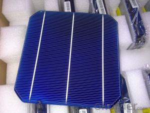


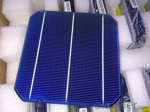


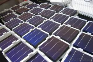
Silicon Wafer in Solar Cell - High Quality A Grade Mono Crystalline 5V 18.0% Solar Cell
- Ref Price:
-

- Loading Port:
- Shanghai
- Payment Terms:
- TT OR LC
- Min Order Qty:
- 1000 pc
- Supply Capability:
- 100000 pc/month
OKorder Service Pledge
OKorder Financial Service
You Might Also Like


Specifications
hot sale solar cell
1.16.8%~18.25% high efficiency
2.100% checked quality
3.ISO9001/ISO14001/TUV/CE/UL
4.stable performance
We can offer you the best quality products and services, don't miss !
POLY6'(156*156)
Polycrystalline Silicon Solar cell
Physical Characteristics
Dimension: 156mm×156mm±0.5mm
Diagonal: 220mm±0.5mm
Thickness(Si): 200±20 μm
Front(-) Back(+)
Blue anti-reflecting coating (silicon nitride); Aluminum back surface field;
1.5mm wide bus bars; 2.0mm wide soldering pads;
Distance between bus bars: 51mm . Distance between bus bars :51mm .
Electrical Characteristics
Efficiency(%) | 18.00 | 17.80 | 17.60 | 17.40 | 17.20 | 16.80 | 16.60 | 16.40 | 16.20 | 16.00 | 15.80 | 15.60 |
Pmpp(W) | 4.33 | 4.29 | 4.24 | 4.19 | 4.14 | 4.09 | 4.04 | 3.99 | 3.94 | 3.90 | 3.86 | 3.82 |
Umpp(V) | 0.530 | 0.527 | 0.524 | 0.521 | 0.518 | 0.516 | 0.514 | 0.511 | 0.509 | 0.506 | 0.503 | 0.501 |
Impp(A) | 8.159 | 8.126 | 8.081 | 8.035 | 7.990 | 7.938 | 7.876 | 7.813 | 7.754 | 7.698 | 7.642 | 7.586 |
Uoc(V) | 0.633 | 0.631 | 0.628 | 0.625 | 0.623 | 0.620 | 0.618 | 0.617 | 0.615 | 0.613 | 0.611 | 0.609 |
Isc(A) | 8.709 | 8.677 | 8.629 | 8.578 | 8.531 | 8.478 | 8.419 | 8.356 | 8.289 | 8.220 | 8.151 | 8.083 |

MONO5'(125*125mm)165
Monocrystalline silicon solar cell
Physical Characteristics
Dimension: 125mm×125mm±0.5mm
Diagonal: 165mm±0.5mm
Thickness(Si): 200±20 μm
Front(-) Back(+)
Blue anti-reflecting coating(silicon nitride); Aluminum back surface field;
1.6mmwide bus bars; 2.5mm wide soldering pads;
Distance between bus bars: 61mm . Distance between bus bars :61mm .
Electrical Characteristics
Efficiency(%) | 19.40 | 19.20 | 19.00 | 18.80 | 18.60 | 18.40 | 18.20 | 18.00 | 17.80 | 17.60 | 17.40 | 17.20 |
Pmpp(W) | 2.97 | 2.94 | 2.91 | 2.88 | 2.85 | 2.82 | 2.79 | 2.76 | 2.73 | 2.70 | 2.67 | 2.62 |
Umpp(V) | 0.537 | 0.535 | 0.533 | 0.531 | 0.527 | 0.524 | 0.521 | 0.518 | 0.516 | 0.515 | 0.513 | 0.509 |
Impp(A) | 5.531 | 5.495 | 5.460 | 5.424 | 5.408 | 5.382 | 5.355 | 5.328 | 5.291 | 5.243 | 5.195 | 4.147 |
Uoc(V) | 0.637 | 0.637 | 0.636 | 0.635 | 0.633 | 0.630 | 0.629 | 0.629 | 0.628 | 0.626 | 0.626 | 0.625 |
Isc(A) | 5.888 | 5.876 | 5.862 | 5.848 | 5.839 | 5.826 | 5.809 | 5.791 | 5.779 | 5.756 | 5.293 | 5.144 |

FAQ:
Q:How can i get some sample?
A:Yes , if you want order ,sample is not a problem.
Q:How about your solar panel efficency?
A: Our product efficency around 17.25%~18.25%.
Q:What’s the certificate you have got?
A: we have overall product certificate of ISO9001/ISO14001/CE/TUV/UL
- Q: What is the purpose of a grounding wire in a solar silicon wafer?
- The purpose of a grounding wire in a solar silicon wafer is to provide a safe path for electrical currents to flow in the event of a fault or malfunction. It helps to prevent electric shocks, fires, and damage to equipment by redirecting any excess electrical current directly to the ground, ensuring the safety of both the solar wafer and the surrounding environment.
- Q: How do solar silicon wafers contribute to sustainable development goals?
- Solar silicon wafers contribute significantly to sustainable development goals by enabling the production of clean and renewable energy. As the key component in solar panels, these wafers harness the power of the sun to generate electricity, reducing the reliance on fossil fuels and mitigating climate change. Solar energy promotes environmental sustainability by reducing greenhouse gas emissions, improving air quality, and conserving valuable natural resources. Additionally, the deployment of solar silicon wafers promotes economic growth, creates job opportunities, and enhances energy access, especially in remote and underdeveloped regions. Overall, solar silicon wafers play a crucial role in achieving sustainable development goals by advancing the transition towards a low-carbon and more resilient energy future.
- Q: How are solar silicon wafers protected from physical damage?
- Solar silicon wafers are typically protected from physical damage through various methods such as encapsulation in protective materials like glass, polymers, or ceramics. Additionally, they may be coated with anti-reflective and anti-scratch coatings to enhance durability. These protective measures safeguard the fragile silicon wafers from breakage, moisture, dust, and other potential sources of physical damage, ensuring their long-term functionality and efficiency in solar panels.
- Q: What are the different wafer orientations used in solar silicon wafer production?
- There are three main wafer orientations used in solar silicon wafer production: <100>, <111>, and <110>. The <100> orientation is the most commonly used, as it provides a balance between cost, efficiency, and ease of production. The <111> orientation is known for its high efficiency, but it is less commonly used due to its higher cost and more complex manufacturing process. The <110> orientation is used in specific applications where superior mechanical strength is required. Overall, the choice of wafer orientation depends on the desired balance between cost, efficiency, and specific application requirements.
- Q: What is the thickness of the semiconductor wafer used today?I have consulted some for solar wafers, heard now that the wafer thickness in 200~400 micron, but we need the wafer thickness requirements for high now, that for semiconductor wafer thickness is slightly higher than the solar energy, but I do not know how much is there in about 1 mm
- For integrated circuits: generally 4 inch wafer thickness of 0.520mm, the thickness of the 6 inch wafer
- Q: Process flow of wafer wafer ultrasonic cleaning machine?
- Plasma cleaning method, which is characterized in that the process parameters of gas flushing process is: the chamber pressure of 15 mTorr, process gas flow 300sccm, time 3S; process parameters of starting process is: the chamber pressure of 15 mTorr, process gas flow on the electrode 300sccm, power 300W, time Ss
- Q: Can solar silicon wafers be used in solar-powered air conditioners?
- Yes, solar silicon wafers can be used in solar-powered air conditioners. Solar silicon wafers are a key component in the production of solar cells, which convert sunlight into electricity. Solar-powered air conditioners utilize this electricity to power their cooling systems, making them energy-efficient and environmentally friendly.
- Q: What is the role of doping in solar silicon wafers?
- Doping plays a critical role in solar silicon wafers as it introduces impurities to control the conductivity and enhance the efficiency of the wafers. By doping the silicon with elements like phosphorus or boron, the electrical properties of the wafer can be altered, allowing for the creation of p-type and n-type regions necessary for the formation of a functional solar cell. This controlled doping helps in the generation and separation of electron-hole pairs, enabling the conversion of sunlight into electricity.
- Q: How do solar silicon wafers handle temperature variations?
- Solar silicon wafers are designed to handle temperature variations quite well. This is because they are typically made from high-quality materials that have been carefully engineered to withstand extreme temperatures. The wafers have a low coefficient of thermal expansion, meaning they expand and contract minimally with temperature changes. This helps to prevent cracking or damage to the wafers. Additionally, solar cells are often encapsulated in protective materials that provide insulation and help regulate temperature, further enhancing their ability to handle temperature variations.
- Q: How are solar silicon wafers protected from extreme temperatures?
- Solar silicon wafers are protected from extreme temperatures by encapsulating them in various layers of protective materials such as glass or polymer. These protective layers act as a barrier, shielding the wafers from direct exposure to high temperatures and preventing any damage or degradation. Additionally, solar panels are designed with proper thermal management systems, including heat sinks and ventilation, to dissipate excess heat and maintain optimal operating temperatures for the silicon wafers.
Send your message to us
Silicon Wafer in Solar Cell - High Quality A Grade Mono Crystalline 5V 18.0% Solar Cell
- Ref Price:
-
- Loading Port:
- Shanghai
- Payment Terms:
- TT OR LC
- Min Order Qty:
- 1000 pc
- Supply Capability:
- 100000 pc/month
OKorder Service Pledge
OKorder Financial Service
Similar products


Hot products


Hot Searches
Related keywords

