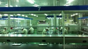
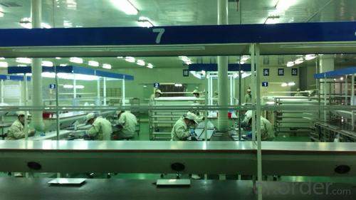


Ic Grade Solar Silicon Wafer Supplier - High Quality A Grade Mono Crystalline 5V 17.8% Solar Cell
- Ref Price:
-

- Loading Port:
- Shanghai
- Payment Terms:
- TT OR LC
- Min Order Qty:
- 1000 pc
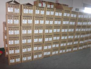
- Supply Capability:
- 100000 pc/month
OKorder Service Pledge
OKorder Financial Service
You Might Also Like


Specifications
hot sale solar cell
1.16.8%~18.25% high efficiency
2.100% checked quality
3.ISO9001/ISO14001/TUV/CE/UL
4.stable performance
We can offer you the best quality products and services, don't miss !
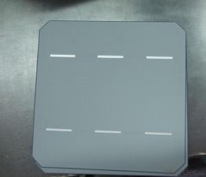
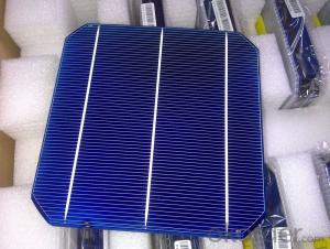
POLY6'(156*156)
Polycrystalline Silicon Solar cell
Physical Characteristics
Dimension: 156mm×156mm±0.5mm
Diagonal: 220mm±0.5mm
Thickness(Si): 200±20 μm
Front(-) Back(+)
Blue anti-reflecting coating (silicon nitride); Aluminum back surface field;
1.5mm wide bus bars; 2.0mm wide soldering pads;
Distance between bus bars: 51mm . Distance between bus bars :51mm .
Electrical Characteristics
Efficiency(%) | 18.00 | 17.80 | 17.60 | 17.40 | 17.20 | 16.80 | 16.60 | 16.40 | 16.20 | 16.00 | 15.80 | 15.60 |
Pmpp(W) | 4.33 | 4.29 | 4.24 | 4.19 | 4.14 | 4.09 | 4.04 | 3.99 | 3.94 | 3.90 | 3.86 | 3.82 |
Umpp(V) | 0.530 | 0.527 | 0.524 | 0.521 | 0.518 | 0.516 | 0.514 | 0.511 | 0.509 | 0.506 | 0.503 | 0.501 |
Impp(A) | 8.159 | 8.126 | 8.081 | 8.035 | 7.990 | 7.938 | 7.876 | 7.813 | 7.754 | 7.698 | 7.642 | 7.586 |
Uoc(V) | 0.633 | 0.631 | 0.628 | 0.625 | 0.623 | 0.620 | 0.618 | 0.617 | 0.615 | 0.613 | 0.611 | 0.609 |
Isc(A) | 8.709 | 8.677 | 8.629 | 8.578 | 8.531 | 8.478 | 8.419 | 8.356 | 8.289 | 8.220 | 8.151 | 8.083 |

MONO5'(125*125mm)165
Monocrystalline silicon solar cell
Physical Characteristics
Dimension: 125mm×125mm±0.5mm
Diagonal: 165mm±0.5mm
Thickness(Si): 200±20 μm
Front(-) Back(+)
Blue anti-reflecting coating(silicon nitride); Aluminum back surface field;
1.6mmwide bus bars; 2.5mm wide soldering pads;
Distance between bus bars: 61mm . Distance between bus bars :61mm .
Electrical Characteristics
Efficiency(%) | 19.40 | 19.20 | 19.00 | 18.80 | 18.60 | 18.40 | 18.20 | 18.00 | 17.80 | 17.60 | 17.40 | 17.20 |
Pmpp(W) | 2.97 | 2.94 | 2.91 | 2.88 | 2.85 | 2.82 | 2.79 | 2.76 | 2.73 | 2.70 | 2.67 | 2.62 |
Umpp(V) | 0.537 | 0.535 | 0.533 | 0.531 | 0.527 | 0.524 | 0.521 | 0.518 | 0.516 | 0.515 | 0.513 | 0.509 |
Impp(A) | 5.531 | 5.495 | 5.460 | 5.424 | 5.408 | 5.382 | 5.355 | 5.328 | 5.291 | 5.243 | 5.195 | 4.147 |
Uoc(V) | 0.637 | 0.637 | 0.636 | 0.635 | 0.633 | 0.630 | 0.629 | 0.629 | 0.628 | 0.626 | 0.626 | 0.625 |
Isc(A) | 5.888 | 5.876 | 5.862 | 5.848 | 5.839 | 5.826 | 5.809 | 5.791 | 5.779 | 5.756 | 5.293 | 5.144 |

FAQ:
Q:How can i get some sample?
A:Yes , if you want order ,sample is not a problem.
Q:How about your solar panel efficency?
A: Our product efficency around 17.25%~18.25%.
Q:What’s the certificate you have got?
A: we have overall product certificate of ISO9001/ISO14001/CE/TUV/UL
- Q: What is the typical warranty period for a solar silicon wafer?
- The typical warranty period for a solar silicon wafer can vary depending on the manufacturer, but it is commonly around 25 to 30 years.
- Q: Development trend of monocrystalline silicon wafer
- Speaking of silicon, we have to mention Chinese LDK! The world's largest manufacturer of solar wafers - Jiangxi LDK LDK Solar Co. Ltd., announced in September 20, 2008, the company has been successful in the United States on a day before the issuance of 4 million 800 thousand shares of American Depositary Shares (ADS), for the price of $41.75, to raise funds of $200 million, mainly for polysilicon plant and wafer factory expansion.It is reported that LDK LDK will use 60% of the net proceeds of the issuance of the company to support the construction of polysilicon plant, the use of polysilicon to expand the production capacity of 30%, for the general business activities of 10%.
- Q: Can solar silicon wafers be used in solar-powered transportation systems?
- Yes, solar silicon wafers can be used in solar-powered transportation systems. They are commonly used in the production of solar panels, which can be installed on vehicles to harness solar energy and power the transportation systems.
- Q: Can solar silicon wafers be used in remote or isolated areas?
- Yes, solar silicon wafers can be used in remote or isolated areas. Solar panels made from silicon wafers can generate electricity from sunlight, making them an ideal solution for areas where access to traditional power grids is limited or non-existent. The modular nature of solar panels allows for easy installation and scalability, making it feasible to meet the energy needs of remote or isolated communities. Additionally, advancements in battery storage technology enable the storage of excess energy generated during the day for use during nighttime or cloudy periods, further enhancing the viability of solar power in remote areas.
- Q: How are solar silicon wafers cut from a silicon ingot?
- Solar silicon wafers are typically cut from a silicon ingot using a wire saw or a diamond-blade saw. The ingot is first sliced into thin wafers using a wire saw that consists of a continuous loop of wire with diamond particles. The wire saw is guided through the ingot, creating multiple wafers simultaneously. Alternatively, a diamond-blade saw can be used, which involves cutting the ingot into wafers with a rotating blade coated with diamond particles. Both methods ensure precise and clean cuts, resulting in the formation of individual solar silicon wafers.
- Q: Why should the wafer cut side, cut out edge Jiaosha
- In fact, early silicon is not cutting edge, but with the development of microelectronics industry began the following reasons: cutting edge, W2) i: J n$W% L* M1 s `&;1, n can do a plurality of microelectronic devices on the wafer, cut down, and there is a crystal to crystal growth requirements, cutting along a direction for cutting chaos crack, cleavage is the professional said. The cutting edge tells you the direction of cleavage.2, N type and P type silicon wafer, a standard trimming is also inform you that it is n type or P type electrical characteristics, electrical characteristics, u$J2 z/ h 9 - O3, microelectronics production has been automated, such as lithography exposure if there is no cutting edge positioning, then the mask plate and the chip will be a difference of 180 degrees or a certain location, production efficiency will be very low...,4, the use of a lot of silicon, in addition to n/p also have crystal direction, for example, do MEMS requires corrosion anisotropy will be used <110> crystal direction, and MOS products in order to reduce the influence of the surface state requirements with <100> crystal...
- Q: How does the doping process affect the performance of a solar silicon wafer?
- The doping process significantly affects the performance of a solar silicon wafer. Doping involves introducing impurities into the silicon crystal lattice to alter its electrical properties. By adding specific elements like boron or phosphorus, the wafer's conductivity can be controlled, enabling the efficient movement of charge carriers. This helps in the creation of p-n junctions, essential for solar cell operation. Doping also enhances the wafer's ability to absorb light, resulting in improved conversion of sunlight into electricity. Overall, the doping process plays a crucial role in optimizing the performance and efficiency of a solar silicon wafer.
- Q: What is the difference between silicon wafer P111 and P100
- <111> is the coordinate of the direction vector<111> is expressed over the origin and point x = 1, y = 1, Z =1 on a straight line passing through the atom
- Q: What is the expected efficiency improvement for multi-junction perovskite-silicon solar silicon wafers?
- The expected efficiency improvement for multi-junction perovskite-silicon solar silicon wafers is significant. These wafers have the potential to achieve much higher efficiencies compared to traditional silicon solar cells. With the combination of perovskite and silicon materials, the multi-junction design allows for better absorption of a wider range of wavelengths, leading to increased energy conversion. Although the exact improvement may vary depending on the specific design and manufacturing processes, it is anticipated that multi-junction perovskite-silicon solar silicon wafers could potentially achieve efficiencies beyond 30% or even higher.
- Q: How are solar silicon wafers etched to enhance light absorption?
- Solar silicon wafers are etched using various techniques, such as chemical etching or texturization, to enhance light absorption. This involves creating a rough surface on the wafer, which helps to reduce reflection and increase the amount of light that is absorbed by the silicon material. By etching the wafer, the surface area is increased, allowing for more interactions between incoming light and the silicon, ultimately improving the efficiency of the solar cell.
Send your message to us
Ic Grade Solar Silicon Wafer Supplier - High Quality A Grade Mono Crystalline 5V 17.8% Solar Cell
- Ref Price:
-
- Loading Port:
- Shanghai
- Payment Terms:
- TT OR LC
- Min Order Qty:
- 1000 pc
- Supply Capability:
- 100000 pc/month
OKorder Service Pledge
OKorder Financial Service
Similar products


Hot products


Hot Searches
Related keywords

