


Solar Silicon Wafer Price - 6 inch 3bb Monocrystalline Best Solar Cell 18.0%
- Ref Price:
-

- Loading Port:
- Shanghai
- Payment Terms:
- TT OR LC
- Min Order Qty:
- 1000 pc
- Supply Capability:
- 100000 pc/month
OKorder Service Pledge
OKorder Financial Service
You Might Also Like


Quick Details
Place of Origin: | China (Mainland) | Brand Name: | xrsolar | Model Number: | ERC-156M-3BB |
Material: | Monocrystalline Silicon | Size: | 6 inch | Number of Cells: | 1 |
Max. Power: | 4.3W | Material:: | monocrystalline Silicon | Size:: | 156mmx156mm or 6 inch |
Max. Power:: | 4.3 watts | efficiency:: | 16%-17.8% | busbar:: | 3 |
Color: | Dark Blue | Voltage:: | 0.508V-0.53V | Thickness:: | 190um±20um |
Packaging & Delivery
Packaging Details: | 100pcs in one box,1000pcs per carton, standard export carton |
Delivery Detail: | 5-7 days after received the payment |
Specifications
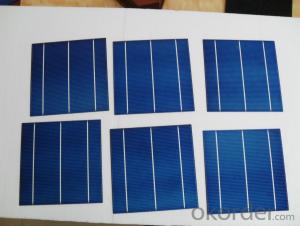
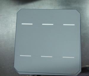
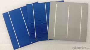
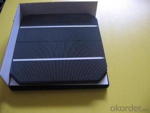
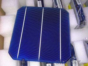
3BB Monocrystallin Best Solar Cell Price
1.Size: 6*6 solar cell
2. Efficiency:4.3WMonocrystallin Best Solar Cell Price
6 Inch 3BB Monocrystallin Best Solar Cell Price
Dimension: 156mm x 156mm
Diagonal: 200mm (round chamfers)
Front: Anisotropically texturized surface and dark silicon nitride
anti-reflection coating
1.9mm silver busbars
Back: Full-surface aluminum back-surface field
4.0mm (silver / aluminum) continuous soldering pads
Features
1.High conversion efficiencies resulting in superior power output performance.
2.Outstanding power output even in low light or high temperature conditions
3.Optimized design for ease of soldering and lamination
4.Long-term stability,reliability and performance
5.Low breakage rate
6.Color uniformaity
Packaging & Shipping
1. Item are only shipped after PAYMENT is received.
2. Originally our solar cells are 100 pieces per box, 10 boxes per carton.
2. Please check out your ADDRESS carefully when processing order.
3. Please CONTACT us ASAP if you haven't received the parcel.
Shipping will be made via EMS, DHL, Fedex, UPS , TNT etc
FAQ:
1. Q: Do you have your own factory?
A: Yes, we have. Our factory located in Jiangsu
2. Q: How can I visit your factory?
A: Before you visit,please contact us.We will show you the route or arrange a car to pick you up.
3. Q: Do you provide free sample?
A: Commenly we provide paid sample.
4. Q: Could you print our company LOGO on the nameplate and package?
A: Yes, we accept it.And need an Authorization Letter from you.


- Q: What is the effect of doping on the bandgap of a solar silicon wafer?
- Doping in a solar silicon wafer has a significant effect on its bandgap. By introducing impurities during the manufacturing process, the bandgap of the silicon wafer can be manipulated to optimize its efficiency as a solar cell. Doping with elements such as phosphorus or boron alters the electrical properties of silicon, widening or narrowing its bandgap accordingly. This adjustment allows the silicon wafer to effectively absorb photons from a broader range of the solar spectrum, enhancing its ability to convert sunlight into electricity. Therefore, doping plays a crucial role in improving the performance and overall efficiency of solar silicon wafers.
- Q: Why do you want to make the wafer bigger? The bigger the better, why?
- The cost of the chip is directly related to the area. On the same chip, the more chips can be carved, the lower the price of the chip. Because silicon chips are inevitably produced defects (such as impurities, etc.). The larger the area of a chip, the higher the probability of the collision, and the higher the proportion of the whole wafer. A chip to do one hundred chips, a defect is 1\%. If only do ten, out of a defect is 10\%. An extreme example is the large CCD, professional camera or digital camera with the CCD is 23.7x15.6mm, light by the light area of 370 square millimeters, quickly catch up with the area of the high-end RISC processor
- Q: Can solar silicon wafers be used in solar-powered data centers?
- Yes, solar silicon wafers can be used in solar-powered data centers. These wafers are the primary material used in the production of solar panels, which generate electricity from sunlight. By incorporating solar panels made from silicon wafers, data centers can harness solar energy to power their operations, reducing reliance on traditional energy sources and promoting sustainability.
- Q: What is the expected efficiency improvement for tandem perovskite-silicon solar silicon wafers?
- The expected efficiency improvement for tandem perovskite-silicon solar silicon wafers is significant, potentially reaching beyond 30%.
- Q: What's the connection between silicon wafer and wafer
- The bigger the chip the smaller the less waste the less the cost. His direct use is of course on Si for mixed metal precipitation until different packaging lithography, as raw materials for the preparation of electronic manufacturing
- Q: Why the resistivity of silicon wafer is high and low
- For example, after heating resistance and cooling, more or less there will be changes in the normal temperature change, is allowed error.
- Q: What is the size of a standard solar silicon wafer?
- A standard solar silicon wafer typically measures around 156mm in diameter.
- Q: Can solar silicon wafers be used in marine or offshore applications?
- Yes, solar silicon wafers can be used in marine or offshore applications. However, special considerations need to be taken into account to ensure their durability and protection against harsh marine environments, such as corrosion resistance and waterproofing. Additionally, marine or offshore solar installations may require specific mounting and anchoring techniques to withstand the challenges posed by waves, saltwater, and high winds.
- Q: Are solar silicon wafers affected by vibrations or shocks?
- Yes, solar silicon wafers can be affected by vibrations or shocks. Excessive vibrations or shocks can cause microcracks, fractures, or dislodgement of the delicate components within the wafer, leading to a decrease in its efficiency or complete failure. It is crucial to handle and transport solar silicon wafers with care to avoid any potential damage.
- Q: Below what the photovoltaic industry specific industry classification, solar silicon manufacturing enterprises, mainly engaged in single and polycrystalline silicon, polycrystalline silicon wafer cutting casting, single enterprise, what are the concrete classification, a solar silicon slice of this industry?
- Photovoltaic involves a lot, but the company makes silicon chips in terms of, so if the use of photovoltaic culvert cover, too general, I need a detailed classification of the industry, and then go to the specific industry analysis
Send your message to us
Solar Silicon Wafer Price - 6 inch 3bb Monocrystalline Best Solar Cell 18.0%
- Ref Price:
-
- Loading Port:
- Shanghai
- Payment Terms:
- TT OR LC
- Min Order Qty:
- 1000 pc
- Supply Capability:
- 100000 pc/month
OKorder Service Pledge
OKorder Financial Service
Similar products


Hot products


Hot Searches
Related keywords

