
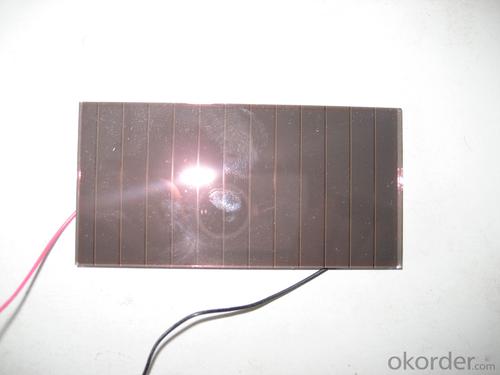
Solar Silicon Wafer - Amorphous Silicon Dice Specification 4
- Ref Price:
-

- Loading Port:
- China Main Port
- Payment Terms:
- TT OR LC
- Min Order Qty:
- -
- Supply Capability:
- -
OKorder Service Pledge
OKorder Financial Service
You Might Also Like


Pv modules at present, the mainstream products are still in silicon as the main raw materials, only in terms of silicon raw material consumption, production 1 mw of crystalline silicon solar cell, need 10 to 12 tons of high purity silicon, but if use the same silicon materials used to produce thin film amorphous silicon solar cell can produce more than 200 mw.
From the perspective of energy consumption, amorphous silicon solar battery only 1-1.5 years of energy recovery period, more embodies its contribution to energy saving in the manufacturing process.
Component occupies a high proportion of costs in a photovoltaic system, the component prices directly affect the system cost, and thus affect the cost of photovoltaic power generation. Calculated at the current price of components, the same money, buy amorphous silicon products, you can get more close to 30% of the power components.
2, more power
For the same power of solar cell array, amorphous silicon solar cell is about 10% more than monocrystalline silicon, polycrystalline silicon battery power. This has been the Uni - Solar System LLC, Energy Photovoltaic Corp., Japan's Kaneka Corp., the Netherlands Energy research institute, and other organizations and experts confirmed that the Photovoltaic industry.
In sunny, that is to say, under the high temperature, amorphous silicon solar cell components can show more excellent power performance.
3, better low light response
Due to the characteristics of amorphous silicon atoms are arranged disorderly, the electron transition no longer comply with the restriction of traditional \"selection rule\", as a result, its light absorption characteristics and there are big differences monocrystalline silicon material. Amorphous silicon and monocrystalline silicon material absorption curve as shown
, amorphous silicon absorption curve has obvious three sections (A, B, C). Area A corresponding electronic transition between localized states, such as the gap state near Fermi level and to the tail state transition, the absorption coefficient is small, about 1-10 cm - 1, for this is absorbing; B area absorption coefficient with the increase of the photon energy index rose, it corresponds to the electrons from the valence band edge extension state to the conduction band localized state transition, as well as the localized electrons from the valence band tail states guide for edge extension state transition, the region's energy range is usually only about half of the electron volts, but absorption coefficient across two or three orders of magnitude, usually up to 104 cm - 1; Area C corresponds to the electrons from the valence band to the conduction band internal internal transition, the absorption coefficient is bigger, often in more than 104 cm - 1. After two absorption area is crystalline silicon eigen absorption area.
Can be seen in the figure, the intersection of two curves about 1.8 ev. It is important to note that in the visible light range (1.7 to 3.0 ev), the absorption coefficient of amorphous silicon material is almost an order of magnitude larger than the single crystal silicon. That is to say, in the morning the first part of the sun is not too strong, the second half, and it's cloudy in the afternoon under the condition of low light intensity, long wave is greater, the amorphous silicon material still has a large absorption coefficient. Again considering the amorphous silicon band gap is larger, the reverse saturation current I0 is smaller. And as mentioned the amorphous silicon battery the characteristics I - V characteristic curve of the amorphous silicon solar cell both in theory and in practical use in low light intensity has good adaptation.
• I - V characteristics of amorphous silicon cells after more than a Vm with the voltage drop slowly
In order to be convenient, we draw the I - V characteristics of two kinds of batteries on the same picture. Crystalline silicon and amorphous silicon battery I - V characteristics of general shape as shown
we see from the picture, two kinds of cells in the curve changes after exceed the maximum output power point gap is bigger. Output current of crystalline silicon cells after exceed the maximum output power point will soon fall to zero, curve steep; Rather than crystalline silicon cells output current after a long distance to fall to zero, the curve is relatively flat. Two kinds of battery Vm equivalent to about 83% of its open circuit voltage and 83% respectively.
when light intensity gradually become hour, short circuit current and open circuit voltage of solar battery will be stronger. Short circuit current decreases faster, of course, open circuit voltage decrease more slowly.
do in battery solar cell array under the condition of load, when the sun battery array of effective output voltage less than the terminal voltage of battery, battery cannot be recharged. When the light intensity gradually become hour, crystal silicon battery charging does not meet the conditions, and amorphous silicon due to the larger voltage difference, do not charge until the light is very dark, effectively increase the use of sunlight time. So, amorphous silicon cells to produce more electricity than the crystalline silicon.
4, more excellent high temperature performance
High in the outdoor environment temperature, amorphous silicon solar cell performance change, depends on the temperature, spectrum, as well as other related factors. But what is certain is: amorphous silicon than monocrystalline silicon or polycrystalline silicon are less likely to be affected by temperature.
Amorphous silicon solar cells than monocrystalline silicon, polycrystalline silicon cells have relatively small temperature coefficient of amorphous silicon solar cell output power best Pm temperature coefficient is about 0.19%, and monocrystalline silicon, polycrystalline silicon cells best output power Pm temperature coefficient is about 0.5%, when the battery work at higher temperatures, the two batteries will be a drop in the Pm, but the decline is different. They can be calculated using the following formula.
- Q: The process for steel wire cutting silicon factory, we use HCTB5 wire, you can do?
- Electroplated diamond wireWith high tensile strength, the strength of electroplated diamond wire is more than 110% of the original strand strength. The technical problem of electroplating line embrittlement caused by plating induced tensile stress is solved successfully.
- Q: What is the expected efficiency improvement for future solar silicon wafers?
- It is difficult to predict an exact number for the expected efficiency improvement of future solar silicon wafers. However, technological advancements and ongoing research suggest that there is potential for significant efficiency improvements in the coming years. With the development of new materials, manufacturing techniques, and advancements in cell architectures, it is expected that solar silicon wafers will continue to become more efficient, allowing for greater conversion of sunlight into electricity.
- Q: Why do you want to make the wafer bigger? The bigger the better, why?
- Because each layer is insulated by silicon dioxide, it is equivalent to a capacitor structure. The larger the span, the greater the capacity of the wiring. The higher the frequency, the more serious side effects such as the integral effect of the long distance transmission. Basically thought GHz must use the following line width.18 technology. Chip size also affects power consumption. With the same mask and the same operating frequency, the smaller the line width, the smaller the voltage. The power consumption is proportional to the square of the voltage. Want to pursue low power you have to honestly narrow the line width. The semiconductor industry in the world are going to kill red eye, if we do not have shortcut yiwofeng to dive in.
- Q: What is the impact of impurities in solar silicon wafers on performance?
- Impurities in solar silicon wafers can have a significant impact on the performance of solar cells. These impurities, such as metal contaminants or dopants, can introduce defects in the crystal structure of the silicon, affecting the efficiency of electron movement and trapping photons. This can lead to reduced power output, decreased conversion efficiency, and shorter lifespan of the solar cells. Therefore, it is crucial to minimize impurities during the manufacturing process to optimize the performance and overall quality of solar silicon wafers.
- Q: Can solar silicon wafers be used in remote or isolated areas?
- Yes, solar silicon wafers can be used in remote or isolated areas. Solar panels made from silicon wafers can generate electricity from sunlight, making them an ideal solution for areas where access to traditional power grids is limited or non-existent. The modular nature of solar panels allows for easy installation and scalability, making it feasible to meet the energy needs of remote or isolated communities. Additionally, advancements in battery storage technology enable the storage of excess energy generated during the day for use during nighttime or cloudy periods, further enhancing the viability of solar power in remote areas.
- Q: The higher the resistivity of silicon wafers, the better?!!! 1 experts please answer me!
- The resistivity is as narrow as possible, high resistance and low resistance can have high efficiency, is stable, easy to make a smooth PN junction in the diffusion resistance, high in the junction zone will less less complex, but more difficult to do the PN junction intact, low resistance lifetime will be shorter, but the PN junction will do very smooth, the higher resistivity is not the main, mainly has the corresponding process to match, want to have a stable process with stable resistivity.
- Q: How do solar silicon wafers handle extreme weather conditions like hailstorms?
- Solar silicon wafers are designed to withstand extreme weather conditions, including hailstorms. They are typically made from highly durable materials such as tempered glass or polycrystalline silicon, which have high resistance to impacts. Additionally, these wafers undergo rigorous testing and certification processes to ensure their ability to withstand hailstorms and other harsh weather conditions. The materials used and the manufacturing processes employed make solar silicon wafers capable of effectively handling hailstorms without significant damage or loss of functionality.
- Q: Can solar silicon wafers be used in urban environments for power generation?
- Yes, solar silicon wafers can definitely be used in urban environments for power generation. The compact size and versatility of solar panels allow them to be easily installed on rooftops, buildings, or even integrated into urban infrastructure such as streetlights or bus stops. This enables urban areas to harness solar energy and generate clean and renewable power in a sustainable manner.
- Q: How do solar silicon wafers perform in high-salt environments?
- Solar silicon wafers generally perform well in high-salt environments due to their inherent corrosion resistance. The protective layers and encapsulation used in solar panels help shield the silicon wafers from the corrosive effects of saltwater or high-salt environments, ensuring their long-term functionality and durability.
- Q: Can solar silicon wafers be used in water desalination plants?
- Yes, solar silicon wafers can be used in water desalination plants. They can be utilized as a component in solar panels to generate electricity, which can then be used to power the desalination process.
Send your message to us
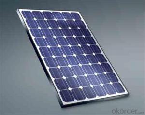
Solar Silicon Wafer - Amorphous Silicon Dice Specification 4
- Ref Price:
-
- Loading Port:
- China Main Port
- Payment Terms:
- TT OR LC
- Min Order Qty:
- -
- Supply Capability:
- -
OKorder Service Pledge
OKorder Financial Service
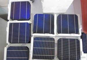
Similar products


Hot products


Hot Searches
Related keywords

