


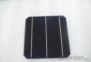
Silicon Wafer Solar Cell Panels - High Quality A Grade Mono Crystalline 5V 18.4% Solar Cells
- Ref Price:
-

- Loading Port:
- Shanghai
- Payment Terms:
- TT OR LC
- Min Order Qty:
- 1000 pc
- Supply Capability:
- 100000 pc/month
OKorder Service Pledge
OKorder Financial Service
You Might Also Like


Specifications
hot sale solar cell
1.16.8%~18.25% high efficiency
2.100% checked quality
3.ISO9001/ISO14001/TUV/CE/UL
4.stable performance
We can offer you the best quality products and services, don't miss !
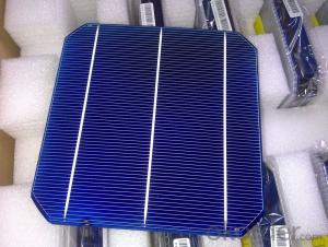
POLY6'(156*156)
Polycrystalline Silicon Solar cell
Physical Characteristics
Dimension: 156mm×156mm±0.5mm
Diagonal: 220mm±0.5mm
Thickness(Si): 200±20 μm
Front(-) Back(+)
Blue anti-reflecting coating (silicon nitride); Aluminum back surface field;
1.5mm wide bus bars; 2.0mm wide soldering pads;
Distance between bus bars: 51mm . Distance between bus bars :51mm .
Electrical Characteristics
Efficiency(%) | 18.00 | 17.80 | 17.60 | 17.40 | 17.20 | 16.80 | 16.60 | 16.40 | 16.20 | 16.00 | 15.80 | 15.60 |
Pmpp(W) | 4.33 | 4.29 | 4.24 | 4.19 | 4.14 | 4.09 | 4.04 | 3.99 | 3.94 | 3.90 | 3.86 | 3.82 |
Umpp(V) | 0.530 | 0.527 | 0.524 | 0.521 | 0.518 | 0.516 | 0.514 | 0.511 | 0.509 | 0.506 | 0.503 | 0.501 |
Impp(A) | 8.159 | 8.126 | 8.081 | 8.035 | 7.990 | 7.938 | 7.876 | 7.813 | 7.754 | 7.698 | 7.642 | 7.586 |
Uoc(V) | 0.633 | 0.631 | 0.628 | 0.625 | 0.623 | 0.620 | 0.618 | 0.617 | 0.615 | 0.613 | 0.611 | 0.609 |
Isc(A) | 8.709 | 8.677 | 8.629 | 8.578 | 8.531 | 8.478 | 8.419 | 8.356 | 8.289 | 8.220 | 8.151 | 8.083 |

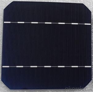
MONO5'(125*125mm)165
Monocrystalline silicon solar cell
Physical Characteristics
Dimension: 125mm×125mm±0.5mm
Diagonal: 165mm±0.5mm
Thickness(Si): 200±20 μm
Front(-) Back(+)
Blue anti-reflecting coating(silicon nitride); Aluminum back surface field;
1.6mmwide bus bars; 2.5mm wide soldering pads;
Distance between bus bars: 61mm . Distance between bus bars :61mm .
Electrical Characteristics
Efficiency(%) | 19.40 | 19.20 | 19.00 | 18.80 | 18.60 | 18.40 | 18.20 | 18.00 | 17.80 | 17.60 | 17.40 | 17.20 |
Pmpp(W) | 2.97 | 2.94 | 2.91 | 2.88 | 2.85 | 2.82 | 2.79 | 2.76 | 2.73 | 2.70 | 2.67 | 2.62 |
Umpp(V) | 0.537 | 0.535 | 0.533 | 0.531 | 0.527 | 0.524 | 0.521 | 0.518 | 0.516 | 0.515 | 0.513 | 0.509 |
Impp(A) | 5.531 | 5.495 | 5.460 | 5.424 | 5.408 | 5.382 | 5.355 | 5.328 | 5.291 | 5.243 | 5.195 | 4.147 |
Uoc(V) | 0.637 | 0.637 | 0.636 | 0.635 | 0.633 | 0.630 | 0.629 | 0.629 | 0.628 | 0.626 | 0.626 | 0.625 |
Isc(A) | 5.888 | 5.876 | 5.862 | 5.848 | 5.839 | 5.826 | 5.809 | 5.791 | 5.779 | 5.756 | 5.293 | 5.144 |

FAQ:
Q:How can i get some sample?
A:Yes , if you want order ,sample is not a problem.
Q:How about your solar panel efficency?
A: Our product efficency around 17.25%~18.25%.
Q:What’s the certificate you have got?
A: we have overall product certificate of ISO9001/ISO14001/CE/TUV/UL
- Q: How are solar silicon wafers connected in a solar panel?
- Solar silicon wafers are typically connected in a solar panel through a process called stringing and tabbing. In this process, the wafers are interconnected using thin conductive wires or ribbons, known as busbars, which create a series circuit. These busbars are soldered onto the front and back contacts of the wafers, allowing for the flow of electricity between them. This interconnected network of wafers forms the photovoltaic module or solar panel.
- Q: What are the different manufacturing processes for solar silicon wafers?
- There are mainly two manufacturing processes for solar silicon wafers: the Czochralski (CZ) process and the Float Zone (FZ) process. In the CZ process, a silicon crystal is grown from a molten silicon melt using a seed crystal, which is then sliced into wafers. The FZ process involves slowly pulling a silicon crystal through a molten zone, creating a solid silicon cylinder that is then sliced into wafers. Both processes require further steps such as wafer polishing and cleaning to produce high-quality solar silicon wafers.
- Q: What is the expected degradation rate of solar silicon wafers over time?
- The expected degradation rate of solar silicon wafers over time varies depending on various factors such as the quality of the silicon material, manufacturing process, environmental conditions, and maintenance practices. However, on average, silicon solar wafers experience a degradation rate of around 0.5-1% per year. This means that after 25 to 30 years, solar panels may have lost around 20-30% of their original efficiency. It's important to note that advancements in technology and improved manufacturing processes are continuously reducing degradation rates, ultimately increasing the lifespan and efficiency of solar panels.
- Q: What is the role of the back contact on a solar silicon wafer?
- The role of the back contact on a solar silicon wafer is to provide a pathway for the flow of current generated by the sun's energy. It helps in collecting and conducting the electrical current produced by the solar cells towards the external circuit. Additionally, the back contact also serves as a reflective layer, minimizing the loss of light and ensuring maximum efficiency in converting solar energy into electricity.
- Q: Can solar silicon wafers be used in solar-powered medical devices?
- Yes, solar silicon wafers can be used in solar-powered medical devices. Solar silicon wafers are commonly used in solar panels to convert sunlight into electricity, and this electricity can be utilized to power various medical devices, including those used in remote or off-grid areas. By harnessing solar energy, these devices can operate independently without relying on traditional power sources, making them more sustainable and accessible in diverse healthcare settings.
- Q: What is the role of back surface field (BSF) on solar silicon wafers?
- The role of the back surface field (BSF) on solar silicon wafers is to reduce the recombination of charge carriers at the rear surface of the wafer. This is achieved by creating a high concentration of dopant atoms at the back surface, which forms a gradient that helps to separate the photo-generated carriers from the rear surface. The BSF also increases the efficiency of the solar cell by improving the collection of charge carriers and reducing the energy losses due to recombination.
- Q: What is the difference between the purpose of wafer cleaning and the cleaning of silicon material, what is the difference between the acid used
- A technique used to reduce the reflectivity of silicon, which is cleaned only by hydrofluoric acid
- Q: What are the different materials used for front contacts in solar silicon wafers?
- The different materials used for front contacts in solar silicon wafers include silver, aluminum, and copper. These materials are chosen for their electrical conductivity and compatibility with the silicon wafer, allowing for efficient collection and transport of the generated solar energy.
- Q: What's the difference between a silicon wafer and a battery?
- Silicon wafers are cut into pieces by wire cutting!The battery pack is a silicon wafer through the surface flocking, diffusion of PN junction, and then PECVD coating
- Q: Can solar silicon wafers be repaired if damaged?
- No, solar silicon wafers cannot be repaired if they are damaged. Once a silicon wafer used for solar cells is damaged, it cannot be fixed or repaired. It is usually more cost-effective and efficient to replace the damaged wafer with a new one.
Send your message to us
Silicon Wafer Solar Cell Panels - High Quality A Grade Mono Crystalline 5V 18.4% Solar Cells
- Ref Price:
-
- Loading Port:
- Shanghai
- Payment Terms:
- TT OR LC
- Min Order Qty:
- 1000 pc
- Supply Capability:
- 100000 pc/month
OKorder Service Pledge
OKorder Financial Service
Similar products


Hot products


Hot Searches
Related keywords

