


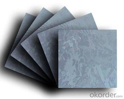

Silicon Solar Wafer
- Ref Price:
-

- Loading Port:
- China Main Port
- Payment Terms:
- TT OR LC
- Min Order Qty:
- -
- Supply Capability:
- -
OKorder Service Pledge
Quality Product, Order Online Tracking, Timely Delivery
OKorder Financial Service
Credit Rating, Credit Services, Credit Purchasing
You Might Also Like


Specifications
IC grade mono silicon wafer
1.Used in various discrete devices
2.High Purity 11N
3.Growth Method :CZ
![]()
| IC grade mono silicon wafer | ||
| Size | 4"/5"/6" | |
| Growth method | CZ | |
| Grade | Prime grade | |
| Diameter | 100±0.4mm / 125±0.5mm / 150±0.5mm | |
| Orientation | <111>/<100> | |
| Type | N-type/P-type | |
| Dopant | P-type:Boron | |
| N-type:Phos./As./Sb. | ||
| Purity | 11N(99.999999999%) | |
| Oxygen Content | ≤18 New PPMA | |
| Carborn Content | ≤1 New PPMA | |
| Resistivity | ≥0.001Ω·cm | |
| Thickness | ≥200um, or according to your requirement | |
| Others | TTV≤10um, Bow≤35um,Warp≤35um | |
| Particles | ≥0.3um@≤10PPW | |
| Surface | Frond side polished,back side etched. | |
| MOQ | 100pcs | |
| Package | Packed in cassette,and sealed in vacuum bag,25pcs/cassette. | |
| Price | According to your specification,especially resistivity and thickness | |


- Q: What is the expected efficiency improvement for future solar silicon wafers?
- It is difficult to predict an exact number for the expected efficiency improvement of future solar silicon wafers. However, technological advancements and ongoing research suggest that there is potential for significant efficiency improvements in the coming years. With the development of new materials, manufacturing techniques, and advancements in cell architectures, it is expected that solar silicon wafers will continue to become more efficient, allowing for greater conversion of sunlight into electricity.
- Q: How do solar silicon wafers perform in high wind conditions?
- Solar silicon wafers are designed to withstand high wind conditions. They are typically mounted securely on frames or structures that are engineered to resist wind loads. Additionally, solar panels undergo rigorous testing to ensure their durability and stability in various environmental conditions, including high winds. Therefore, solar silicon wafers perform well and maintain their functionality even in high wind conditions.
- Q: What is the role of back surface field on solar silicon wafers?
- The back surface field on solar silicon wafers plays a crucial role in enhancing the overall efficiency of solar cells. It acts as a reflective layer that helps to prevent the recombination of charge carriers at the back surface of the wafer. This reduces the loss of current and improves the collection of photons, resulting in higher power output from the solar cell. Additionally, the back surface field also aids in reducing the surface recombination velocity, which further enhances the performance and stability of the solar cell.
- Q: How are solar silicon wafers packaged and shipped?
- Solar silicon wafers are typically packaged and shipped in protective containers or trays. These containers are designed to securely hold the wafers in place and protect them from damage during transportation. The wafers are carefully stacked in the packaging with appropriate spacing to prevent any contact or scratching. Additionally, the packaging may include layers of foam or other cushioning materials to provide further protection. Once packaged, the wafers are typically shipped in bulk using suitable shipping methods, such as air freight or specialized carriers, to ensure safe delivery to their destination.
- Q: How is the wafer appearance caused? The performance of the chip half white, a class of black! Seek help!
- You should be the color difference problem is caused by the mortar temperature cutting room temperature and workshop temperature also influenced to reduce this effect only from the cleaning rod to minimize the time spent between, this is the enthusiasm of the staff problem
- Q: What are the different materials used for passivation layers in solar silicon wafers?
- The different materials used for passivation layers in solar silicon wafers include silicon nitride (SiNx), aluminum oxide (Al2O3), and silicon oxide (SiO2). These materials are applied as thin films on the surface of the wafers to enhance their energy conversion efficiency and protect them from external factors such as moisture and contamination.
- Q: Are there any advancements in solar silicon wafer surface texturing techniques?
- Yes, there have been significant advancements in solar silicon wafer surface texturing techniques. Researchers and industry experts have been continuously working on improving the efficiency and performance of solar cells, and one area of focus has been the texture of silicon wafers. Various texturing techniques like chemical etching, laser processing, and plasma techniques have been developed to enhance light trapping and reduce reflection, ultimately increasing the overall efficiency of solar cells. These advancements in surface texturing techniques have played a crucial role in the development of more efficient and cost-effective solar panels.
- Q: What are the dimensions of a standard solar silicon wafer?
- The dimensions of a standard solar silicon wafer are typically around 156mm in size, with a thickness of around 200 micrometers.
- Q: How do solar silicon wafers compare to other types of solar cell technologies?
- Solar silicon wafers are the most widely used and established technology in the solar cell industry. They offer high efficiency and reliability, making them a preferred choice for many applications. Compared to other types of solar cell technologies like thin-film or organic cells, silicon wafers generally have higher conversion efficiencies and longer lifespans. However, they are also more expensive to manufacture and require more material, which can limit their suitability for certain applications. Overall, solar silicon wafers remain a reliable and efficient option for harnessing solar energy.
- Q: How are defects in solar silicon wafers detected?
- Defects in solar silicon wafers are typically detected using various techniques such as visual inspection, infrared imaging, and electrical testing. Visual inspection involves examining the wafer's surface for visible imperfections, such as cracks, scratches, or impurities. Infrared imaging can identify defects by measuring the heat distribution across the wafer, as irregularities often generate different thermal patterns. Electrical testing is conducted by applying a voltage or current to the wafer and analyzing its response to identify any anomalies or abnormalities. These techniques allow manufacturers to identify and remove defective wafers, ensuring the production of high-quality solar cells.
Send your message to us
Silicon Solar Wafer
- Ref Price:
-
- Loading Port:
- China Main Port
- Payment Terms:
- TT OR LC
- Min Order Qty:
- -
- Supply Capability:
- -
OKorder Service Pledge
Quality Product, Order Online Tracking, Timely Delivery
OKorder Financial Service
Credit Rating, Credit Services, Credit Purchasing
Similar products


Hot products


Hot Searches

