


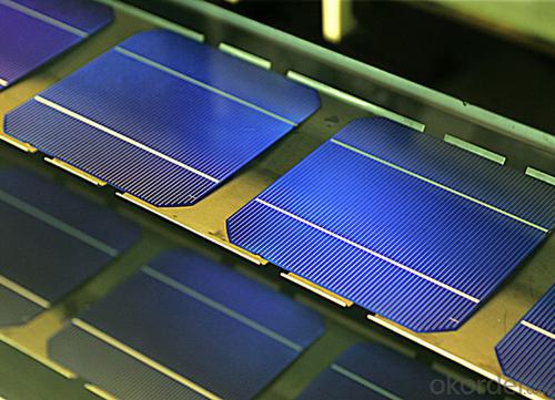


Multicrystalline Silicon Solar Wafer - High Quality A Grade Polycrystalline 5V 17.8% Solar Cell
- Ref Price:
-

- Loading Port:
- Shanghai
- Payment Terms:
- TT OR LC
- Min Order Qty:
- 1000 pc
- Supply Capability:
- 100000 pc/month
OKorder Service Pledge
OKorder Financial Service
You Might Also Like


Specifications
hot sale solar cell
1.16.8%~18.25% high efficiency
2.100% checked quality
3.ISO9001/ISO14001/TUV/CE/UL
4.stable performance
We can offer you the best quality products and services, don't miss !
POLY6'(156*156)
Polycrystalline Silicon Solar cell
Physical Characteristics
Dimension: 156mm×156mm±0.5mm
Diagonal: 220mm±0.5mm
Thickness(Si): 200±20 μm
Front(-) Back(+)
Blue anti-reflecting coating (silicon nitride); Aluminum back surface field;
1.5mm wide bus bars; 2.0mm wide soldering pads;
Distance between bus bars: 51mm . Distance between bus bars :51mm .
Electrical Characteristics
Efficiency(%) | 18.00 | 17.80 | 17.60 | 17.40 | 17.20 | 16.80 | 16.60 | 16.40 | 16.20 | 16.00 | 15.80 | 15.60 |
Pmpp(W) | 4.33 | 4.29 | 4.24 | 4.19 | 4.14 | 4.09 | 4.04 | 3.99 | 3.94 | 3.90 | 3.86 | 3.82 |
Umpp(V) | 0.530 | 0.527 | 0.524 | 0.521 | 0.518 | 0.516 | 0.514 | 0.511 | 0.509 | 0.506 | 0.503 | 0.501 |
Impp(A) | 8.159 | 8.126 | 8.081 | 8.035 | 7.990 | 7.938 | 7.876 | 7.813 | 7.754 | 7.698 | 7.642 | 7.586 |
Uoc(V) | 0.633 | 0.631 | 0.628 | 0.625 | 0.623 | 0.620 | 0.618 | 0.617 | 0.615 | 0.613 | 0.611 | 0.609 |
Isc(A) | 8.709 | 8.677 | 8.629 | 8.578 | 8.531 | 8.478 | 8.419 | 8.356 | 8.289 | 8.220 | 8.151 | 8.083 |

MONO5'(125*125mm)165
Monocrystalline silicon solar cell
Physical Characteristics
Dimension: 125mm×125mm±0.5mm
Diagonal: 165mm±0.5mm
Thickness(Si): 200±20 μm
Front(-) Back(+)
Blue anti-reflecting coating(silicon nitride); Aluminum back surface field;
1.6mmwide bus bars; 2.5mm wide soldering pads;
Distance between bus bars: 61mm . Distance between bus bars :61mm .
Electrical Characteristics
Efficiency(%) | 19.40 | 19.20 | 19.00 | 18.80 | 18.60 | 18.40 | 18.20 | 18.00 | 17.80 | 17.60 | 17.40 | 17.20 |
Pmpp(W) | 2.97 | 2.94 | 2.91 | 2.88 | 2.85 | 2.82 | 2.79 | 2.76 | 2.73 | 2.70 | 2.67 | 2.62 |
Umpp(V) | 0.537 | 0.535 | 0.533 | 0.531 | 0.527 | 0.524 | 0.521 | 0.518 | 0.516 | 0.515 | 0.513 | 0.509 |
Impp(A) | 5.531 | 5.495 | 5.460 | 5.424 | 5.408 | 5.382 | 5.355 | 5.328 | 5.291 | 5.243 | 5.195 | 4.147 |
Uoc(V) | 0.637 | 0.637 | 0.636 | 0.635 | 0.633 | 0.630 | 0.629 | 0.629 | 0.628 | 0.626 | 0.626 | 0.625 |
Isc(A) | 5.888 | 5.876 | 5.862 | 5.848 | 5.839 | 5.826 | 5.809 | 5.791 | 5.779 | 5.756 | 5.293 | 5.144 |

FAQ:
Q:How can i get some sample?
A:Yes , if you want order ,sample is not a problem.
Q:How about your solar panel efficency?
A: Our product efficency around 17.25%~18.25%.
Q:What’s the certificate you have got?
A: we have overall product certificate of ISO9001/ISO14001/CE/TUV/UL
- Q: What is the impact of temperature on the performance of solar silicon wafers?
- The performance of solar silicon wafers is significantly affected by temperature. Higher temperatures can lead to a decrease in the efficiency of solar cells, causing a reduction in power output. This is primarily due to the increase in resistive losses and the decrease in the voltage of the solar cells at higher temperatures. Additionally, excessive heat can degrade the materials used in solar cells, leading to a decline in their overall performance and lifespan. Therefore, maintaining optimal operating temperatures is crucial for maximizing the efficiency and longevity of solar silicon wafers.
- Q: Can solar silicon wafers be used in solar-powered smart cities?
- Yes, solar silicon wafers can be used in solar-powered smart cities. Silicon wafers are the most common material used in solar panels to convert sunlight into electricity. As solar power is a key component of smart cities, these wafers can be utilized to generate clean and sustainable energy for various applications and infrastructure within such cities.
- Q: What is a silicon wafer for unidirectional and bidirectional cutting? What is the difference between the two?
- The cutting line is cut in one direction, and the wire is cut into the waste wire wheel from the discharge wheel
- Q: How is a power output measured in a solar silicon wafer?
- The power output of a solar silicon wafer is typically measured by using a solar simulator to expose the wafer to a controlled light source. The electrical current generated by the wafer is then measured using a current-voltage (IV) curve tracer or a solar cell tester. The power output is calculated by multiplying the current and voltage values obtained from the measurements.
- Q: How do solar silicon wafers perform in areas with limited sunlight?
- Solar silicon wafers do not perform as efficiently in areas with limited sunlight. The amount of sunlight directly affects the amount of energy the solar panel can generate. Therefore, in areas with limited sunlight, the performance of solar silicon wafers will be reduced, resulting in lower energy production.
- Q: Seeking for the video: manual insert silicon wafer single crystal insert method
- To solve the finger print is very simple, as long as the requirements of employees can not in the whole process of operation of the silicon bare hand contact can be, no debris is not possible, but to see the machine or man-made debris or before the procedure is cracked as, if it is man-made debris, to do a a standard specification, as long as the control that would reduce the rate of fragmentation. Or artificial debris to staff assessment, but also meet the results. I used to track debris for a long time, when all of the pieces are controlled by the descendants of the debris is very low. The main road is the most hidden crack. If the semi automatic equipment under normal circumstances will not produce debris, such as automatic equipment, such as degumming equipment will produce debris, mainly the spray pressure is too large, but the pressure is also very little fragmentation of the right. I think the main thing is to see if you have asked the staff how to do it, followed by the implementation of your employees are required. You can look at these lines on the line!
- Q: What is the expected efficiency improvement for quantum dot solar silicon wafers?
- The expected efficiency improvement for quantum dot solar silicon wafers is significant, with some studies suggesting a potential enhancement of up to 50% compared to traditional silicon solar cells.
- Q: What are the main manufacturers of solar silicon wafers?
- Some of the main manufacturers of solar silicon wafers include companies like Wacker Chemie AG, Shin-Etsu Chemical Co., Ltd., and REC Silicon ASA. These companies are known for their expertise in producing high-quality silicon wafers that are used in the manufacturing of solar panels.
- Q: What is the role of oxide layers on solar silicon wafers?
- The role of oxide layers on solar silicon wafers is to passivate the surface of the wafer and reduce recombination of charge carriers, thereby improving the efficiency of the solar cell.
- Q: How is a grounding wire connected to a solar silicon wafer?
- A grounding wire is typically connected to a solar silicon wafer through a conductive adhesive or soldering. The wire is securely attached to the wafer's metallic frame or a designated grounding point on the solar panel, ensuring a direct path for any electrical charges to safely dissipate into the ground, reducing the risk of electrical hazards.
Send your message to us
Multicrystalline Silicon Solar Wafer - High Quality A Grade Polycrystalline 5V 17.8% Solar Cell
- Ref Price:
-
- Loading Port:
- Shanghai
- Payment Terms:
- TT OR LC
- Min Order Qty:
- 1000 pc
- Supply Capability:
- 100000 pc/month
OKorder Service Pledge
OKorder Financial Service
Similar products


Hot products


Hot Searches
Related keywords

