

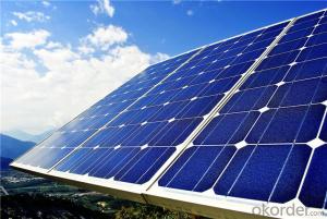
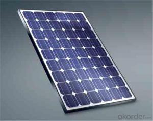
250W Solar Silicon Wafer Panels for Home Use Solar Power System
- Ref Price:
-

- Loading Port:
- China main port
- Payment Terms:
- TT OR LC
- Min Order Qty:
- 10000 watt
- Supply Capability:
- 20000000 watt/month
OKorder Service Pledge
OKorder Financial Service
You Might Also Like


Destription:
Solar panel refers to a panel designed to absorb the sun's rays as a source of energy for generating electricity or heating. A PV module is a packaged, connected assembly of typically 6×10 solar cells. Solar PV panels constitute the solar array of a photovoltaic system that generates and supplies solar electricity in commercial and residential applications.
Main Characteristic
1.Manufactured according to international quality and Environment Management
System (ISO9001, ISO14001)
2. By the high transmittance, low iron tempered glass, anti-aging of the EVA(polyethylene - vinyl acetate), high-performance crystalline silicon solar cells, good Weather resistance TPT (fluoroplastics composite membrane) by pyramid , has a good Weather resistance and anti-UV, hail, water-proof capacity.
3. OEM and customerized package are accepted
4. High efficiency crystalline silicon solar cells
Quality warranty
1.10 years limited warranty on material and workmanship
2. more than 90% power output in 10 years
3. more than 80% power output in 25 years
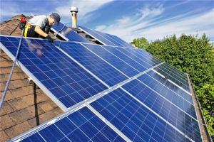
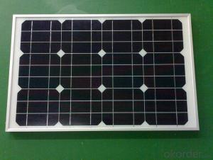
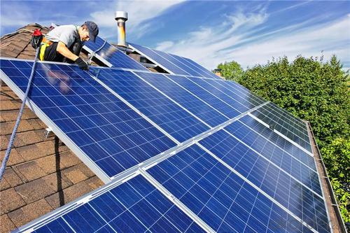
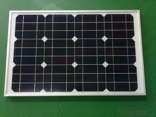
Product show


- Q: What is the role of surface passivation on solar silicon wafers?
- The role of surface passivation on solar silicon wafers is to improve the efficiency and performance of the solar cells. Passivation involves the application of a thin layer of material on the surface of the silicon wafer to reduce surface recombination, which is the loss of electrons and holes at the surface. This helps to minimize the loss of charge carriers and improves the overall electrical properties of the solar cell. By reducing surface recombination, surface passivation increases the conversion efficiency of the solar cell and enhances its ability to generate electricity from sunlight.
- Q: Can solar silicon wafers be used in harsh climates?
- Yes, solar silicon wafers can be used in harsh climates. They are designed to withstand various environmental conditions, including extreme temperatures, humidity, and even exposure to dust and sand. Additionally, solar panels are tested and certified to ensure their durability and performance in harsh climates, making them suitable for use in such environments.
- Q: What is the role of surface recombination velocity on solar silicon wafers?
- The surface recombination velocity on solar silicon wafers plays a crucial role in determining the efficiency of solar cells. It represents the rate at which charge carriers (electrons and holes) recombine at the surface of the wafer. A low surface recombination velocity is desirable as it reduces the recombination losses, allowing more charge carriers to reach the contacts and contribute to the electricity generation. Therefore, optimizing and minimizing the surface recombination velocity is essential for improving the performance of solar cells and increasing their overall efficiency.
- Q: What is the typical efficiency degradation rate of a solar silicon wafer over time?
- The typical efficiency degradation rate of a solar silicon wafer over time is around 0.5% to 1% per year.
- Q: How are solar silicon wafers protected from physical damage?
- Solar silicon wafers are typically protected from physical damage through various methods such as encapsulation in protective materials like glass, polymers, or ceramics. Additionally, they may be coated with anti-reflective and anti-scratch coatings to enhance durability. These protective measures safeguard the fragile silicon wafers from breakage, moisture, dust, and other potential sources of physical damage, ensuring their long-term functionality and efficiency in solar panels.
- Q: Can solar silicon wafers be used in concentrated photovoltaics (CPV)?
- Yes, solar silicon wafers can be used in concentrated photovoltaics (CPV) systems. CPV systems use lenses or mirrors to concentrate sunlight onto solar cells, increasing their efficiency. While CPV typically relies on multi-junction solar cells, which are more efficient than traditional silicon-based solar cells, silicon wafers can still be used in CPV systems to generate electricity.
- Q: How are solar silicon wafers handled and stored to prevent contamination?
- Solar silicon wafers are typically handled and stored in cleanroom environments to prevent contamination. These cleanrooms maintain controlled temperature, humidity, and air quality levels to minimize the presence of particles and pollutants. The wafers are usually stored in sealed containers or cassettes to protect them from dust, moisture, and other contaminants. Additionally, operators and technicians wear protective clothing, such as gloves and coveralls, to avoid direct contact and potential contamination of the wafers.
- Q: What is the role of back surface field in solar silicon wafers?
- The back surface field in solar silicon wafers helps to enhance the efficiency of solar cells by reducing the recombination of charge carriers. It creates a strong electric field at the back surface of the wafer, which prevents the loss of electrons and holes, thereby improving the overall performance of the solar cell.
- Q: Can solar silicon wafers be used in underwater solar energy systems?
- Yes, solar silicon wafers can be used in underwater solar energy systems. However, special precautions need to be taken to ensure the wafers are properly sealed to prevent water damage and corrosion. Additionally, the design of the system should consider factors such as buoyancy, water pressure, and maintenance requirements in underwater environments.
- Q: Can solar silicon wafers be made flexible for applications in wearable devices?
- Yes, solar silicon wafers can be made flexible for applications in wearable devices. Advances in technology have allowed for the development of flexible solar cells that use thin-film materials instead of rigid silicon wafers. These flexible solar cells can be integrated into wearable devices, such as smartwatches or clothing, allowing them to generate power from sunlight while maintaining their flexibility and functionality.
Send your message to us
250W Solar Silicon Wafer Panels for Home Use Solar Power System
- Ref Price:
-
- Loading Port:
- China main port
- Payment Terms:
- TT OR LC
- Min Order Qty:
- 10000 watt
- Supply Capability:
- 20000000 watt/month
OKorder Service Pledge
OKorder Financial Service
Similar products

Hot products


Hot Searches
Related keywords

