


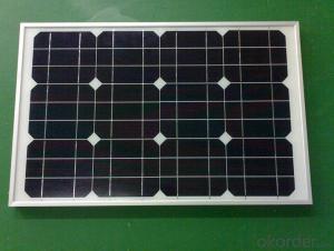
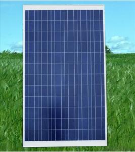
240w Solar Silicon Wafer Carrier Panel for Home Use Solar Power System
- Ref Price:
-

- Loading Port:
- China main port
- Payment Terms:
- TT OR LC
- Min Order Qty:
- 10000 watt
- Supply Capability:
- 20000000 watt/month
OKorder Service Pledge
OKorder Financial Service
You Might Also Like


Destription:
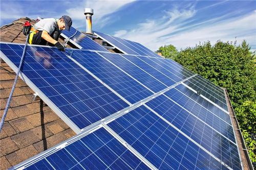
Solar panel refers to a panel designed to absorb the sun's rays as a source of energy for generating electricity or heating. A PV module is a packaged, connected assembly of typically 6×10 solar cells. Solar PV panels constitute the solar array of a photovoltaic system that generates and supplies solar electricity in commercial and residential applications.
Main Characteristic
1.Manufactured according to international quality and Environment Management
System (ISO9001, ISO14001)
2. By the high transmittance, low iron tempered glass, anti-aging of the EVA(polyethylene - vinyl acetate), high-performance crystalline silicon solar cells, good Weather resistance TPT (fluoroplastics composite membrane) by pyramid , has a good Weather resistance and anti-UV, hail, water-proof capacity.
3. OEM and customerized package are accepted
4. High efficiency crystalline silicon solar cells
Quality warranty
1.10 years limited warranty on material and workmanship
2. more than 90% power output in 10 years
3. more than 80% power output in 25 years
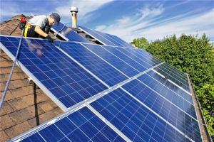
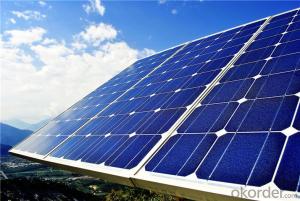
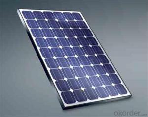
Product show


- Q: How does the quality of a solar silicon wafer affect solar cell performance?
- The quality of a solar silicon wafer significantly affects solar cell performance. A high-quality wafer ensures better efficiency and durability in converting sunlight into electricity. It affects the cell's ability to capture and absorb sunlight, reducing losses due to reflection and recombination of electrons. A low-quality wafer may contain impurities or defects that can hinder the flow of electrons, reducing the overall performance and power output of the solar cell. Therefore, investing in high-quality silicon wafers is crucial for maximizing the efficiency and long-term performance of solar cells.
- Q: Can solar silicon wafers be used in smart grid applications?
- Yes, solar silicon wafers can be used in smart grid applications. Smart grids require efficient and sustainable energy sources, and solar silicon wafers are a key component of solar panels, which are a popular renewable energy solution. By harnessing solar power, these wafers can contribute to the generation of clean electricity for smart grid systems, enabling better energy management, distribution, and integration with advanced technologies.
- Q: What is a silicon chip made of?
- A simple understanding of the silicon wafer is a silicon material cut into pieces by processing. Silicon is a kind of high hardness material, silicon material looks like a stone, he must be washed clean and then heated by a stove melt forming a bulk silicon ingot, and then use the special machine to slice into pieces.
- Q: What is the thickness of the semiconductor wafer used today?I have consulted some for solar wafers, heard now that the wafer thickness in 200~400 micron, but we need the wafer thickness requirements for high now, that for semiconductor wafer thickness is slightly higher than the solar energy, but I do not know how much is there in about 1 mm
- We do DIP package, 4 inch wafer to be thin to 0.300mm; 6 inch wafer to be reduced to about 0.320mm, error 0.020mm.
- Q: How to calculate the conversion efficiency of monocrystalline silicon
- Solar cell efficiency = (open circuit voltage * short-circuit voltage * fill factor) / (battery area * light amplitude) *100%Light intensity - AM1.5 as the standard, that is 1000W/m2Proportion of dark current - Irev>6 cell ratioThe proportion of low efficiency tablets - the proportion of P156Eff<14.5% batteries
- Q: How are solar silicon wafers protected from fire hazards?
- Solar silicon wafers are typically protected from fire hazards through the use of fire-resistant encapsulation materials and manufacturing processes. These encapsulation materials, such as glass or special polymers, provide a protective barrier around the silicon wafer, preventing it from being exposed to direct flame or heat sources. Additionally, stringent quality control measures are implemented during the manufacturing process to ensure that the wafers are not vulnerable to ignition or combustion.
- Q: What is the typical cost per watt for a solar silicon wafer?
- The typical cost per watt for a solar silicon wafer can vary depending on various factors such as quality, quantity, and market conditions. However, as of 2021, the average cost per watt for a solar silicon wafer is around $0.20 to $0.30.
- Q: I would like to ask the solar cell (silicon) production process is the principle of how
- Three, diffusion systemSolar cells require a large area of PN junction to achieve the conversion of light energy to electrical energy, while the diffusion furnace is a special equipment for manufacturing solar cell PN junction. Tube type diffusion furnace is mainly composed of quartz boat download four parts part, gas chamber, a furnace body part and a holder part etc.. Generally, the liquid source of three phosphorus oxychloride is used as the diffusion source. The P type silicon wafer is placed in a quartz tube of a tube type diffusion furnace, and three nitrogen oxychloride is used in the quartz vessel at the temperature of 850---900 degrees Celsius, and the phosphorus atom is obtained through the reaction of the phosphorus oxychloride and the silicon wafer through the reaction of the phosphorus and the phosphorus. After a certain time, the phosphorus atom from the surrounding surface layer into a silicon wafer, and wafer to internal diffusion through the void between the silicon atoms, forming a N type semiconductor and P type semiconductor interface, namely PN junction. The PN junction made by this method has good uniformity, the uniformity of box resistance is less than ten percent, and the lifetime of less than 10ms. The manufacture of PN junction is the most basic and most important process in the production of solar cells. Because it is the formation of PN junction, so that the electrons and holes in the flow is no longer back to the original place, so that the formation of the current, using the wire will lead to the current, dc.
- Q: Are solar silicon wafers affected by lightning strikes?
- Yes, solar silicon wafers can be affected by lightning strikes. Lightning strikes can cause physical damage to solar panels, including the silicon wafers, by melting or cracking them. Additionally, the high electrical currents associated with lightning strikes can potentially damage the electrical components of the solar panel system, such as the inverters. Therefore, it is important for solar panel installations to have proper lightning protection measures in place to minimize the risk of damage.
- Q: How does the efficiency of a solar silicon wafer change with panel orientation?
- The efficiency of a solar silicon wafer can change with panel orientation. The orientation and tilt angle of the solar panel can affect the amount of sunlight it receives, which directly impacts its efficiency. Ideally, a solar panel should be oriented to face the sun directly and tilted at an angle that maximizes sunlight absorption. If the panel is not properly oriented or tilted, it may receive less sunlight, leading to a decrease in efficiency.
Send your message to us
240w Solar Silicon Wafer Carrier Panel for Home Use Solar Power System
- Ref Price:
-
- Loading Port:
- China main port
- Payment Terms:
- TT OR LC
- Min Order Qty:
- 10000 watt
- Supply Capability:
- 20000000 watt/month
OKorder Service Pledge
OKorder Financial Service
Similar products

Hot products


Hot Searches
Related keywords

