


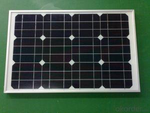
Solar Silicon Wafer Price - High Quality A Grade Polycrystalline 5V 16.0% Solar Cell
- Ref Price:
-

- Loading Port:
- Shanghai
- Payment Terms:
- TT OR LC
- Min Order Qty:
- 1000 pc
- Supply Capability:
- 100000 pc/month
OKorder Service Pledge
OKorder Financial Service
You Might Also Like


Specifications
hot sale solar cell
1.16.8%~18.25% high efficiency
2.100% checked quality
3.ISO9001/ISO14001/TUV/CE/UL
4.stable performance
We can offer you the best quality products and services, don't miss !
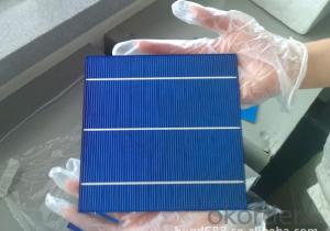
POLY6'(156*156)
Polycrystalline Silicon Solar cell
Physical Characteristics
Dimension: 156mm×156mm±0.5mm
Diagonal: 220mm±0.5mm
Thickness(Si): 200±20 μm
Front(-) Back(+)
Blue anti-reflecting coating (silicon nitride); Aluminum back surface field;
1.5mm wide bus bars; 2.0mm wide soldering pads;
Distance between bus bars: 51mm . Distance between bus bars :51mm .
Electrical Characteristics
Efficiency(%) | 18.00 | 17.80 | 17.60 | 17.40 | 17.20 | 16.80 | 16.60 | 16.40 | 16.20 | 16.00 | 15.80 | 15.60 |
Pmpp(W) | 4.33 | 4.29 | 4.24 | 4.19 | 4.14 | 4.09 | 4.04 | 3.99 | 3.94 | 3.90 | 3.86 | 3.82 |
Umpp(V) | 0.530 | 0.527 | 0.524 | 0.521 | 0.518 | 0.516 | 0.514 | 0.511 | 0.509 | 0.506 | 0.503 | 0.501 |
Impp(A) | 8.159 | 8.126 | 8.081 | 8.035 | 7.990 | 7.938 | 7.876 | 7.813 | 7.754 | 7.698 | 7.642 | 7.586 |
Uoc(V) | 0.633 | 0.631 | 0.628 | 0.625 | 0.623 | 0.620 | 0.618 | 0.617 | 0.615 | 0.613 | 0.611 | 0.609 |
Isc(A) | 8.709 | 8.677 | 8.629 | 8.578 | 8.531 | 8.478 | 8.419 | 8.356 | 8.289 | 8.220 | 8.151 | 8.083 |

MONO5'(125*125mm)165
Monocrystalline silicon solar cell
Physical Characteristics
Dimension: 125mm×125mm±0.5mm
Diagonal: 165mm±0.5mm
Thickness(Si): 200±20 μm
Front(-) Back(+)
Blue anti-reflecting coating(silicon nitride); Aluminum back surface field;
1.6mmwide bus bars; 2.5mm wide soldering pads;
Distance between bus bars: 61mm . Distance between bus bars :61mm .
Electrical Characteristics
Efficiency(%) | 19.40 | 19.20 | 19.00 | 18.80 | 18.60 | 18.40 | 18.20 | 18.00 | 17.80 | 17.60 | 17.40 | 17.20 |
Pmpp(W) | 2.97 | 2.94 | 2.91 | 2.88 | 2.85 | 2.82 | 2.79 | 2.76 | 2.73 | 2.70 | 2.67 | 2.62 |
Umpp(V) | 0.537 | 0.535 | 0.533 | 0.531 | 0.527 | 0.524 | 0.521 | 0.518 | 0.516 | 0.515 | 0.513 | 0.509 |
Impp(A) | 5.531 | 5.495 | 5.460 | 5.424 | 5.408 | 5.382 | 5.355 | 5.328 | 5.291 | 5.243 | 5.195 | 4.147 |
Uoc(V) | 0.637 | 0.637 | 0.636 | 0.635 | 0.633 | 0.630 | 0.629 | 0.629 | 0.628 | 0.626 | 0.626 | 0.625 |
Isc(A) | 5.888 | 5.876 | 5.862 | 5.848 | 5.839 | 5.826 | 5.809 | 5.791 | 5.779 | 5.756 | 5.293 | 5.144 |

FAQ:
Q:How can i get some sample?
A:Yes , if you want order ,sample is not a problem.
Q:How about your solar panel efficency?
A: Our product efficency around 17.25%~18.25%.
Q:What’s the certificate you have got?
A: we have overall product certificate of ISO9001/ISO14001/CE/TUV/UL
- Q: What is the role of surface recombination velocity on solar silicon wafers?
- The surface recombination velocity on solar silicon wafers plays a crucial role in determining the efficiency of solar cells. It represents the rate at which charge carriers (electrons and holes) recombine at the surface of the wafer. A low surface recombination velocity is desirable as it reduces the recombination losses, allowing more charge carriers to reach the contacts and contribute to the electricity generation. Therefore, optimizing and minimizing the surface recombination velocity is essential for improving the performance of solar cells and increasing their overall efficiency.
- Q: Wafer cutting will appear thick sheet, I would like to ask what the reasons are
- Solving measures:A. guide slot check slot is uniform, and to compensate for the loss according to the situation of the slot wheel.When the A. is set to zero, the position of the guide line is controlled.B. standard viscose operation. When the surface of the silicon block is bonded with the guide bar, the utility model can be used to check whether the guide strip is bent, and whether the glue is evenly applied, so that there is no gap between the guide strip and the silicon block after the bonding guide strip is arranged.In the process of using the C. guide wheel, the utility model is used to detect the guide groove of the guide wheel on a regular basis, and the depth and the angle of the guide groove are observed.
- Q: 1 megawatts of solar energy need how many wafers
- Now on the market every piece of the specification is not enough, there are 40W 60W 100W, etc.. One megawatt is equal to 100 watts, yourself.
- Q: Are there any advancements in solar silicon wafer technology?
- Yes, there have been significant advancements in solar silicon wafer technology. Researchers and manufacturers have been working on improving the efficiency and cost-effectiveness of silicon wafers used in solar cells. Some advancements include the development of thin-film silicon wafers, which require less material and energy during production, and the incorporation of new materials and processes to enhance the conversion efficiency of solar cells. These advancements aim to make solar energy more affordable and accessible for a wider range of applications.
- Q: How is the silicon chip integrated circuit?
- Description: the above process is only an example. The name of the process, in the name of different manufacturers have different. But roughly so. There are some differences between the process of MOS circuit and.
- Q: What is the typical weight of a solar silicon wafer?
- The typical weight of a solar silicon wafer is around 5 to 10 grams.
- Q: What is the cost of a solar silicon wafer?
- The cost of a solar silicon wafer can vary depending on several factors such as the size, quality, and quantity being purchased. On average, a standard 156 mm x 156 mm solar silicon wafer can range from $0.10 to $0.30 per piece. However, prices may fluctuate due to market conditions and supplier negotiations.
- Q: Can solar silicon wafers be used in building-integrated photovoltaics (BIPV)?
- Yes, solar silicon wafers can be used in building-integrated photovoltaics (BIPV). BIPV refers to the integration of solar panels or cells into the building envelope, such as windows, roofs, or facades. Silicon wafers are commonly used in the production of solar cells, including those used in BIPV systems. These wafers are processed to create solar cells, which can then be integrated into various building materials, allowing for the generation of solar power while also serving as functional building elements.
- Q: What is the role of a mounting structure in a solar silicon wafer?
- The role of a mounting structure in a solar silicon wafer is to provide support and stability to the wafer, allowing it to be securely attached to a solar panel or other mounting surface. The mounting structure ensures that the wafer is properly positioned and protected, maximizing its exposure to sunlight and optimizing its energy generation capabilities.
- Q: I grew up in the silicon chip Ag particles, the size of about a few hundred nanometers, I would like to ask how I do before the TEM sample?
- Alcohol is usually placed inside, with ultrasonic cleaning instrument scattered about, the purpose is to make the particles do not reunite together.
Send your message to us
Solar Silicon Wafer Price - High Quality A Grade Polycrystalline 5V 16.0% Solar Cell
- Ref Price:
-
- Loading Port:
- Shanghai
- Payment Terms:
- TT OR LC
- Min Order Qty:
- 1000 pc
- Supply Capability:
- 100000 pc/month
OKorder Service Pledge
OKorder Financial Service
Similar products


Hot products


Hot Searches
Related keywords

