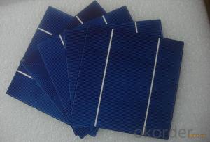


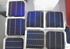
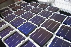
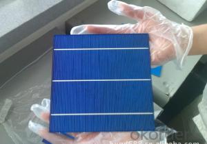
Solar Silicon Wafer Cassette Supplier - High Current 18.0% Polycrystalline Silicon Solar Cell
- Ref Price:
-

- Loading Port:
- Shanghai
- Payment Terms:
- TT OR LC
- Min Order Qty:
- 1000 pc
- Supply Capability:
- 100000 pc/month
OKorder Service Pledge
OKorder Financial Service
You Might Also Like


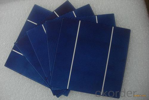
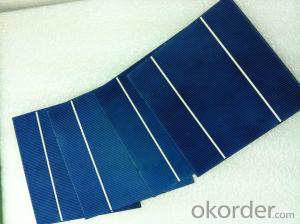
4 Bus Bars 156*156 17.6% efficiency poly solar cell
PHYSICAL CHARACTERISTICS
Dimension: 156mm x 156mm ± 0.5mm
Wafer Thickeness: 180um+20um and 200um+20um
Front(-) Four 1.2mm silver busbar
Silicon nitride blue anti-reflection coating
Back(+) aluminum back surface field
1.75mm(silver) wide segment soldering pads

Typical Electrical Characteristics
Efficiency | W(Pmpp) | V(Umpp) | A(Impp) | V(Uoc) | A(Isc) |
17.4-17.5 | 4.234 | 0.517 | 8.231 | 0.622 | 8.759 |
17.5-17.6 | 4.259 | 0.519 | 8.243 | 0.623 | 8.769 |
17.7-17.8 | 4.283 | 0.521 | 8.256 | 0.625 | 8.779 |
17.8-17.9 | 4.307 | 0.523 | 8.268 | 0.626 | 8.788 |
17.9-18.0 | 4.332 | 0.525 | 8.281 | 0.627 | 8.798 |
18.0-18.1 | 4.380 | 0.529 | 8.306 | 0.629 | 8.808 |
18.1-18.2 | 4.405 | 0.531 | 8.318 | 0.632 | 8.818 |
18.2-18.3 | 4.429 | 0.533 | 8.331 | 0.633 | 8.837 |
18.3-18.4 | 4.453 | 0.535 | 8.344 | 0.634 | 8.847 |
18.4-18.5 | 4.478 | 0.537 | 8.356 | 0.636 | 8.856 |
18.5-18.6 | 4.502 | 0.539 | 8.369 | 0.637 | 8.866 |
Efficiency | W(Pmpp) | V(Umpp) | A(Impp) | V(Uoc) | A(Isc) |
20.90-21.00 | 5.06 | 0.557 | 9.007 | 0.653 | 9.688 |
20.80-20.90 | 5.04 | 0.556 | 9.062 | 0.652 | 9.683 |
20.70-20.80 | 5.02 | 0.554 | 9.055 | 0.651 | 9.684 |
20.60-20.70 | 4.99 | 0.552 | 9.033 | 0.651 | 9.672 |
20.50-20.60 | 4.97 | 0.550 | 9.002 | 0.650 | 9.673 |
20.40-20.50 | 4.94 | 0.548 | 9.012 | 0.649 | 9.674 |
20.30-20.40 | 4.92 | 0.546 | 9.009 | 0.649 | 9.655 |
20.20-20.30 | 4.89 | 0.543 | 9.012 | 0.648 | 9.634 |
20.10-20.20 | 4.87 | 0.541 | 8.998 | 0.648 | 9.617 |
20.00-20.10 | 4.85 | 0.540 | 8.977 | 0.647 | 9.600 |
*Data under standard testing conditional (STC):1,000w/m2,AM1.5, 25°C , Pmax:Positive power tolerance.
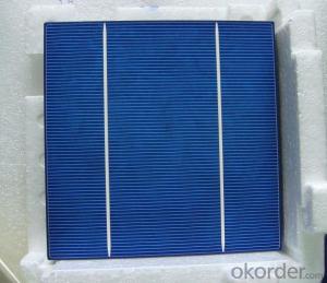
3 Bus Bars 156*156 17.4% efficiency poly solar cell
Dimension: 156 mm x 156 mm ± 0.5 mm
Wafer Thickeness: 156 mm x 156 mm ± 0.5 mm

Typical Electrical Characteristics:
| Efficiency code | 1660 | 1680 | 1700 | 1720 | 1740 | 1760 | 1780 | 1800 | 1820 | 1840 | 1860 |
| Efficiency (%) | 16.6 | 16.8 | 17.0 | 17.2 | 17.4 | 17.6 | 17.8 | 18.0 | 18.2 | 18.4 | 18.6 |
| Pmax (W) | 4.04 | 4.09 | 4.14 | 4.19 | 4.23 | 4.28 | 4.33 | 4.38 | 4.43 | 4.48 | 4.53 |
| Voc (V) | 0.612 | 0.615 | 0.618 | 0.621 | 0.624 | 0.627 | 0.629 | 0.63 | 0.633 | 0.635 | 0.637 |
| Isc (A) | 8.42 | 8.46 | 8.51 | 8.56 | 8.61 | 8.65 | 8.69 | 8.73 | 8.77 | 8.81 | 8.84 |
| Imp (A) | 7.91 | 7.99 | 8.08 | 8.16 | 8.22 | 8.27 | 8.33 | 8.38 | 8.43 | 8.48 | 8.53 |
* Testing conditions: 1000 W/m2, AM 1.5, 25 °C, Tolerance: Efficiency ± 0.2% abs., Pmpp ±1.5% rel.
* Imin : at 0.5 V
Production:

Package:

FAQ:
1. Q: Do you have your own factory?
A: Yes, we have. Our factory located in Jiangsu
2. Q: How can I visit your factory?
A: Before you visit,please contact us.We will show you the route or arrange a car to pick you up.
3. Q: Do you provide free sample?
A: Commenly we provide paid sample.
4. Q: Could you print our company LOGO on the nameplate and package?
A: Yes, we accept it.And need an Authorization Letter from you.
5. Q: Do you accept custom design on size?
A: Yes, if the size is reasonable.
6. Q: How can I be your agent in my country?
A: Please leave feedback. It's better for us to talk about details by email.
7. Q: Do you have solar project engineer who can guide me to install system?
A: Yes, we have a professional engineer team. They can teach you how to install a solar system.
- Q: What is the impact of temperature on the performance of solar silicon wafers?
- The performance of solar silicon wafers is significantly affected by temperature. Higher temperatures can lead to a decrease in the efficiency of solar cells, causing a reduction in power output. This is primarily due to the increase in resistive losses and the decrease in the voltage of the solar cells at higher temperatures. Additionally, excessive heat can degrade the materials used in solar cells, leading to a decline in their overall performance and lifespan. Therefore, maintaining optimal operating temperatures is crucial for maximizing the efficiency and longevity of solar silicon wafers.
- Q: What is the role of a junction box connector in a solar silicon wafer?
- The role of a junction box connector in a solar silicon wafer is to provide a secure and efficient electrical connection between the solar cells on the wafer and the external circuitry. It acts as a junction point where the individual solar cells are connected in series or parallel to form a complete solar module. The junction box connector also ensures protection against environmental factors such as moisture and dust, and may include diodes to prevent reverse current flow.
- Q: Can solar silicon wafers be used in space heating systems?
- Yes, solar silicon wafers can be used in space heating systems. When sunlight hits the silicon wafers, it generates electricity through the photovoltaic effect. This electricity can be used to power space heating systems, either directly or by storing it in batteries for later use.
- Q: What are the reasons for the emergence of the black chip phenomenon of the monocrystalline silicon, which aspects of the production process have an impact on it, preventive measures, and improvement measures?
- Or storage time is too long, vacuum packaging problems, the outside world has the dust into the adsorption on the surface of silicon, this will happen. There is the central part of the polishing process, there is a problem of pressure, resulting in the removal of the center is not enough, the surface roughness is very poor, in the semiconductor level light irradiation, the center of the silicon will appear black.
- Q: How are solar silicon wafers protected from thermal shock during manufacturing?
- Solar silicon wafers are protected from thermal shock during manufacturing through several methods. One common approach is to use thermal annealing, where the wafers are gradually heated and cooled to relieve any internal stress and prevent cracking. Additionally, the use of specialized furnaces and controlled heating processes helps ensure a gradual and uniform temperature change, minimizing the risk of thermal shock. Finally, some manufacturers also apply protective coatings or use support materials to provide extra insulation and buffering against rapid temperature changes, further safeguarding the wafers from thermal shock.
- Q: How is an encapsulant applied to a solar silicon wafer?
- An encapsulant is typically applied to a solar silicon wafer through a process called lamination. This involves placing the wafer between two layers of encapsulant material, such as EVA (ethylene-vinyl acetate), and then subjecting it to heat and pressure. The heat melts the encapsulant, enabling it to bond with the wafer, while the pressure ensures uniform distribution of the material and helps to remove any air bubbles. This lamination process provides protection to the solar silicon wafer from environmental factors and enhances its durability and performance.
- Q: What are the different materials used for encapsulants in solar silicon wafers?
- The different materials used for encapsulants in solar silicon wafers include ethylene-vinyl acetate (EVA), polyolefin-based materials, and thermoplastic polyurethane (TPU). These materials are used to provide protection, insulation, and adhesion for the silicon wafers, ensuring their durability and longevity in the harsh environmental conditions.
- Q: What is the role of back surface field (BSF) on solar silicon wafers?
- The role of the back surface field (BSF) on solar silicon wafers is to reduce the recombination of charge carriers at the rear surface of the wafer. This is achieved by creating a high concentration of dopant atoms at the back surface, which forms a gradient that helps to separate the photo-generated carriers from the rear surface. The BSF also increases the efficiency of the solar cell by improving the collection of charge carriers and reducing the energy losses due to recombination.
- Q: What is the reason for the original or the original silicon?
- The complaint can be suppliers, with hydrofluoric acid washed off after processed velvet
- Q: What is the effect of impurities on the performance of solar silicon wafers?
- Impurities have a detrimental effect on the performance of solar silicon wafers. These impurities can interfere with the flow of electrons, reducing the efficiency of the solar cells. They can also cause defects in the crystal lattice structure, leading to decreased electrical conductivity and overall performance of the wafers. Therefore, minimizing impurities is crucial for maximizing the efficiency and reliability of solar silicon wafers.
Send your message to us
Solar Silicon Wafer Cassette Supplier - High Current 18.0% Polycrystalline Silicon Solar Cell
- Ref Price:
-
- Loading Port:
- Shanghai
- Payment Terms:
- TT OR LC
- Min Order Qty:
- 1000 pc
- Supply Capability:
- 100000 pc/month
OKorder Service Pledge
OKorder Financial Service
Similar products

Hot products


Hot Searches
Related keywords

