


Silicon Wafer Solar Panel - High Quality A Grade Mono晶Silicon 5V 18.2% Solar Cell
- Ref Price:
-

- Loading Port:
- Shanghai
- Payment Terms:
- TT OR LC
- Min Order Qty:
- 1000 pc
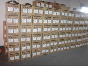
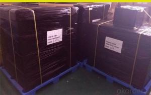
- Supply Capability:
- 100000 pc/month
OKorder Service Pledge
OKorder Financial Service
You Might Also Like


Specifications
hot sale solar cell
1.16.8%~18.25% high efficiency
2.100% checked quality
3.ISO9001/ISO14001/TUV/CE/UL
4.stable performance
We can offer you the best quality products and services, don't miss !
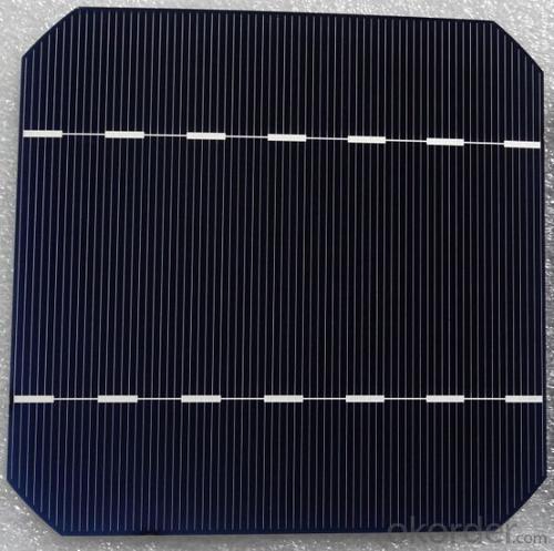
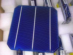
POLY6'(156*156)
Polycrystalline Silicon Solar cell
Physical Characteristics
Dimension: 156mm×156mm±0.5mm
Diagonal: 220mm±0.5mm
Thickness(Si): 200±20 μm
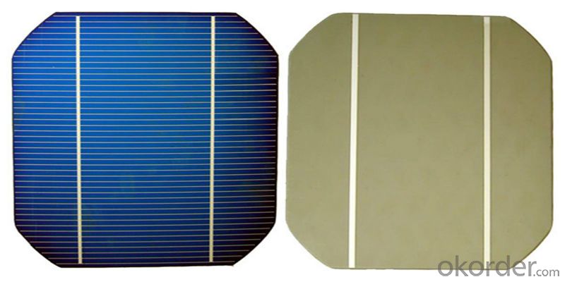
Front(-) Back(+)
Blue anti-reflecting coating (silicon nitride); Aluminum back surface field;
1.5mm wide bus bars; 2.0mm wide soldering pads;
Distance between bus bars: 51mm . Distance between bus bars :51mm .
Electrical Characteristics
Efficiency(%) | 18.00 | 17.80 | 17.60 | 17.40 | 17.20 | 16.80 | 16.60 | 16.40 | 16.20 | 16.00 | 15.80 | 15.60 |
Pmpp(W) | 4.33 | 4.29 | 4.24 | 4.19 | 4.14 | 4.09 | 4.04 | 3.99 | 3.94 | 3.90 | 3.86 | 3.82 |
Umpp(V) | 0.530 | 0.527 | 0.524 | 0.521 | 0.518 | 0.516 | 0.514 | 0.511 | 0.509 | 0.506 | 0.503 | 0.501 |
Impp(A) | 8.159 | 8.126 | 8.081 | 8.035 | 7.990 | 7.938 | 7.876 | 7.813 | 7.754 | 7.698 | 7.642 | 7.586 |
Uoc(V) | 0.633 | 0.631 | 0.628 | 0.625 | 0.623 | 0.620 | 0.618 | 0.617 | 0.615 | 0.613 | 0.611 | 0.609 |
Isc(A) | 8.709 | 8.677 | 8.629 | 8.578 | 8.531 | 8.478 | 8.419 | 8.356 | 8.289 | 8.220 | 8.151 | 8.083 |

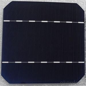
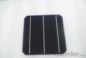
MONO5'(125*125mm)165
Monocrystalline silicon solar cell
Physical Characteristics
Dimension: 125mm×125mm±0.5mm
Diagonal: 165mm±0.5mm
Thickness(Si): 200±20 μm
Front(-) Back(+)
Blue anti-reflecting coating(silicon nitride); Aluminum back surface field;
1.6mmwide bus bars; 2.5mm wide soldering pads;
Distance between bus bars: 61mm . Distance between bus bars :61mm .
Electrical Characteristics
Efficiency(%) | 19.40 | 19.20 | 19.00 | 18.80 | 18.60 | 18.40 | 18.20 | 18.00 | 17.80 | 17.60 | 17.40 | 17.20 |
Pmpp(W) | 2.97 | 2.94 | 2.91 | 2.88 | 2.85 | 2.82 | 2.79 | 2.76 | 2.73 | 2.70 | 2.67 | 2.62 |
Umpp(V) | 0.537 | 0.535 | 0.533 | 0.531 | 0.527 | 0.524 | 0.521 | 0.518 | 0.516 | 0.515 | 0.513 | 0.509 |
Impp(A) | 5.531 | 5.495 | 5.460 | 5.424 | 5.408 | 5.382 | 5.355 | 5.328 | 5.291 | 5.243 | 5.195 | 4.147 |
Uoc(V) | 0.637 | 0.637 | 0.636 | 0.635 | 0.633 | 0.630 | 0.629 | 0.629 | 0.628 | 0.626 | 0.626 | 0.625 |
Isc(A) | 5.888 | 5.876 | 5.862 | 5.848 | 5.839 | 5.826 | 5.809 | 5.791 | 5.779 | 5.756 | 5.293 | 5.144 |

FAQ:
Q:How can i get some sample?
A:Yes , if you want order ,sample is not a problem.
Q:How about your solar panel efficency?
A: Our product efficency around 17.25%~18.25%.
Q:What’s the certificate you have got?
A: we have overall product certificate of ISO9001/ISO14001/CE/TUV/UL
- Q: Can solar silicon wafers be used in solar-powered space vehicles?
- Yes, solar silicon wafers can be used in solar-powered space vehicles. They are commonly used in photovoltaic cells to convert sunlight into electricity, providing a sustainable power source for space missions.
- Q: Why silicon wafers are made in watts! There are several specifications for silicon wafers!
- Battery specifications good variety:103*103mm125*125mm150*150mm156*156mmThe longest seen is the single crystal 125*125mm polycrystalline 156*156mm according to the efficiency to determine the current efficiency of the battery chip is 16%--19%
- Q: Can solar silicon wafers be used in military or defense applications?
- Yes, solar silicon wafers can be used in military or defense applications. They can be integrated into various military equipment and systems such as remote sensors, surveillance systems, unmanned aerial vehicles (UAVs), and portable power systems for soldiers in the field. Solar silicon wafers provide a reliable and sustainable source of power in remote or hostile environments, reducing the dependence on traditional fuel sources and increasing operational capabilities.
- Q: What is the role of a power optimizer in a solar silicon wafer?
- A power optimizer in a solar silicon wafer plays a crucial role in maximizing the energy output from each individual solar panel. It optimizes the performance of the panels by ensuring that each panel operates at its maximum power point, even in cases where panels are affected by shading or mismatched conditions. This helps to increase overall system efficiency, improve energy production, and reduce the impact of factors that may hinder the performance of the solar panels.
- Q: Can solar silicon wafers be damaged by hail or other weather conditions?
- Yes, solar silicon wafers can be damaged by hail or other severe weather conditions. Hailstones can cause physical impact damage, cracking or shattering the wafers, which can affect the efficiency and functionality of solar panels. Additionally, extreme weather conditions like high winds, heavy rain, or lightning strikes can also potentially cause damage to the silicon wafers. Proper installation and protective measures can help mitigate these risks.
- Q: What is the impact of wafer surface quality on solar silicon wafer performance?
- The impact of wafer surface quality on solar silicon wafer performance is significant. A high-quality surface ensures better light absorption, improved electron mobility, and reduced recombination of charge carriers. This leads to higher efficiency and overall performance of the solar cell. Conversely, a poor surface quality can result in reduced light absorption, increased electron recombination, and lower overall efficiency. Therefore, achieving and maintaining a high-quality wafer surface is crucial for optimizing the performance of solar silicon wafers.
- Q: How are solar silicon wafers disposed of at the end of their life cycle?
- Solar silicon wafers are typically recycled at the end of their life cycle. Various recycling methods are employed, including mechanical and chemical processes, to separate and recover valuable materials such as silicon, silver, and glass. These recovered materials can then be reused in the manufacturing of new solar panels or other products, minimizing waste and reducing the environmental impact of the solar industry.
- Q: How are solar silicon wafers affected by surface passivation techniques?
- Surface passivation techniques can significantly improve the performance and efficiency of solar silicon wafers. These techniques involve applying a thin layer of passivating material, such as silicon nitride or aluminum oxide, to the surface of the wafers. This layer helps to reduce the recombination of charge carriers at the surface, which in turn reduces losses and improves the overall efficiency of the solar cell. Additionally, surface passivation techniques also enhance the electrical properties of the solar silicon wafers, leading to better performance and longer lifespan of the solar cells.
- Q: How are solar silicon wafers protected from potential theft?
- Solar silicon wafers are typically protected from potential theft through a combination of security measures. These measures can include physical barriers such as fences, locks, and surveillance cameras to deter unauthorized access. Additionally, solar farms may employ security personnel to monitor the premises and prevent theft. Advanced tracking and monitoring systems can also be installed to detect any suspicious activity and ensure prompt response.
- Q: How is a solar silicon wafer connected to other components in a solar panel?
- A solar silicon wafer is typically connected to other components in a solar panel through a process called soldering. Soldering involves using a soldering iron to melt solder, a metal alloy, and then applying it to the connections between the wafer and other components. This creates a strong electrical and mechanical bond, allowing for efficient transfer of electricity within the solar panel.
Send your message to us
Silicon Wafer Solar Panel - High Quality A Grade Mono晶Silicon 5V 18.2% Solar Cell
- Ref Price:
-
- Loading Port:
- Shanghai
- Payment Terms:
- TT OR LC
- Min Order Qty:
- 1000 pc
- Supply Capability:
- 100000 pc/month
OKorder Service Pledge
OKorder Financial Service
Similar products


Hot products


Hot Searches
Related keywords

