


Silicon Wafer Solar Cell Panels - Monosolicion Poly 156mm*156mm
- Ref Price:
-

- Loading Port:
- China main port
- Payment Terms:
- TT OR LC
- Min Order Qty:
- 100 watt
- Supply Capability:
- 10000 watt/month
OKorder Service Pledge
Quality Product, Order Online Tracking, Timely Delivery
OKorder Financial Service
Credit Rating, Credit Services, Credit Purchasing
You Might Also Like


Monosolicion Solar Cells Poly 156mm*156mm
Typical electrical characteristics
Efficiency code | 1720 | 1740 | 1760 | 1780 | 1820 | 1840 | |
Efficiency (min) | (%) | 17.2 | 17.4 | 17.6 | 17.8 | 18.2 | 18.4 |
Pmax | (W) | 4.186 | 4.234 | 4.283 | 4.332 | 4.429 | 4.478 |
Voc | (V) | 0.631 | 0.632 | 0.634 | 0.636 | 0.640 | 0.642 |
Isc | (A) | 8.446 | 8.485 | 8.523 | 8.573 | 8.660 | 8.700 |
Vmp | (V) | 0.525 | 0.527 | 0.529 | 0.531 | 0.535 | 0.537 |
Imp | (A) | 7.973 | 8.035 | 8.097 | 8.160 | 8.280 | 8.340 |
Data under standard testing conditions(STC): 1,000W/m2, AM1.5, 25℃, Pmax: Positive power tolerance.
Typical teperature coefficients
Voltage | -2.08 | mV/K |
Current | +4.58 | mA/K |
Power | -0.40 | %/K |
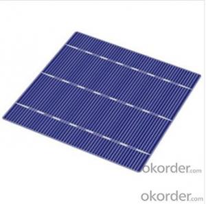
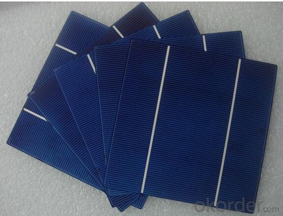
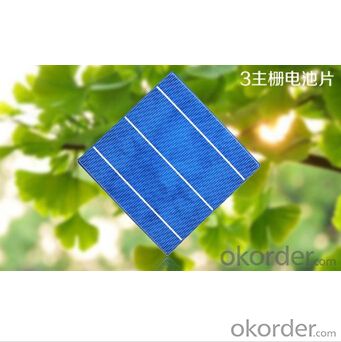
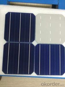
Cell Picture


- Q: How is a power output measured in a solar silicon wafer?
- The power output of a solar silicon wafer is typically measured by connecting it to a load resistance and measuring the voltage and current generated by the wafer. The power output is then calculated by multiplying the voltage and current values.
- Q: What is the role of gettering in solar silicon wafers?
- The role of gettering in solar silicon wafers is to reduce or eliminate impurities and defects that can hinder the performance and efficiency of solar cells. Gettering helps to trap and remove unwanted impurities and contaminants, such as metal impurities and dislocations, from the bulk silicon material. This process ensures that the silicon wafers used in solar cells have a higher purity level, leading to improved electrical conductivity and overall performance of the solar cells.
- Q: Do solar silicon wafers emit any pollutants or greenhouse gases during operation?
- No, solar silicon wafers do not emit any pollutants or greenhouse gases during operation. They are a clean and environmentally friendly source of energy.
- Q: What is the size of a typical solar silicon wafer?
- A typical solar silicon wafer is typically 156 mm (6.14 inches) in size.
- Q: What is the typical size of a solar silicon wafer?
- The typical size of a solar silicon wafer is 156mm x 156mm or 6 inches x 6 inches.
- Q: How to make resistance on a piece of silicon chip (IC)? Read a lot of related articles, but also the first silicon oxidation, in the end is how? Best draw a
- Method for making the Baidu transistor circuit.Simply by laser, and method of mixed batch chemical piling up complex circuit
- Q: What is the expected growth rate for the solar silicon wafer market?
- The expected growth rate for the solar silicon wafer market is projected to be significant, with estimates ranging from 6% to 8% annually.
- Q: What is the surface hardness of monocrystalline silicon and polycrystalline silicon wafers
- At this time, the hardness and elastic modulus of the oxide layer on the surface of monocrystalline silicon wafer were measured, which were about 10.2 GPa and 140.3 GPa, respectively. When the contact depth is about 32 ~ 60NM, silicon wafer contact stiffness and contact depth into a non linear relation between the hardness and elastic modulus increased sharply with the contact depth, show that the hardness and elastic modulus of monocrystalline silicon oxide film surface layer is affected by the matrix material.
- Q: How do solar silicon wafers perform in desert environments?
- Solar silicon wafers perform well in desert environments due to the high levels of sunlight and low humidity. The dry and hot conditions in deserts allow for efficient solar energy generation, as there are fewer obstructions such as clouds or pollution. However, it is important to ensure proper maintenance and cleaning of the wafers to prevent the accumulation of dust or sand particles, which can hinder their performance.
- Q: What is the typical thickness tolerance of a solar silicon wafer?
- The typical thickness tolerance of a solar silicon wafer is around 20-30 micrometers.
Send your message to us
Silicon Wafer Solar Cell Panels - Monosolicion Poly 156mm*156mm
- Ref Price:
-
- Loading Port:
- China main port
- Payment Terms:
- TT OR LC
- Min Order Qty:
- 100 watt
- Supply Capability:
- 10000 watt/month
OKorder Service Pledge
Quality Product, Order Online Tracking, Timely Delivery
OKorder Financial Service
Credit Rating, Credit Services, Credit Purchasing
Similar products


Hot products


Hot Searches
Related keywords

