


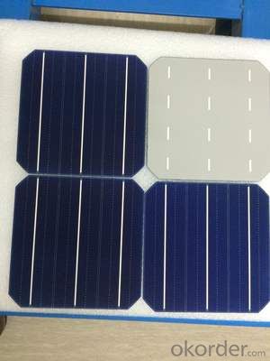
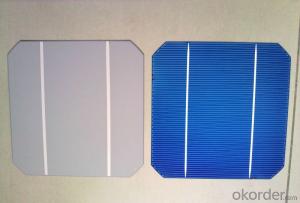
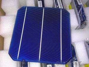
Silicon Wafer in Solar Photovoltaic Cells - Mono Solar Cells 156mm*156mm in Bulk Quantity Low Price Stock 19.8
- Ref Price:
-

- Loading Port:
- Shanghai
- Payment Terms:
- TT OR LC
- Min Order Qty:
- 1000 pc
- Supply Capability:
- 100000 pc/month
OKorder Service Pledge
OKorder Financial Service
You Might Also Like


Brief Introduction
- Up to 20.0% efficiency, one of the highest performing mono crystalline cells on the market
- Three bus bars boosts current collection over the entire cell area, leading to higher fill factors
- Blue anti-reflecting coating allows more sunlight be captured and converted to electricity
- Finer, closer fingers improves charge collections for improved energy yield
- Lower light-induced degradation leads to greater power output over the entire module lifetime
- All solar cells are tightly classified to optimize output of module
- Maximum yield and longevity due to hotspot prevention
- Premium appearance results in a highly uniform and aesthetically appealing module
Specification
- Product Mono-crystalline silicon solar cell
- Dimension 156 mm x 156 mm ± 0.5 mm
- Thickness 200 μm ± 30 μm
- Front 1.5 ± 0.1 mm busbar (silver)
- Silicon nitride antireflection coating
- Back 3.0 mm continuous soldering pads (silver)
- Back surface field (aluminum)
Electric performance parameters

- Testing conditions: 1000 W/m2, AM 1.5, 25 °C, Tolerance: Efficiency ± 0.2% abs., Pmpp ±1.5% rel.
- Imin : at 0.5 V
Light Intensity Dependence

Soldering Ability
- Peel Strength: > 1.0 N/mm (Pull soldered ribbon from busbar in 5 mm/s of 180°)
Dimension Figure

Quick Response
- Any time and anywhere, reply clients' email and solve all problems happen in the work at the first time.
- Remove clients doubts and offer the best solution at the first time.
- Give our clients the lastest news of the photovoltaic, update the newest stock informtion.
Production and Quality Control
- Precision cell efficiency sorting procedures
- Stringent criteria for color uniformity and appearance
- Reverse current and shunt resistance screening
- ISO9001,ISO14001 and OHSAS 18001,TUV Certificated


FAQ:
1. Q: Do you have your own factory?
A: Yes, we have. Our factory located in Jiangsu
2. Q: How can I visit your factory?
A: Before you visit,please contact us.We will show you the route or arrange a car to pick you up.
3. Q: Do you provide free sample?
A: Commenly we provide paid sample.
4. Q: Could you print our company LOGO on the nameplate and package?
A: Yes, we accept it.And need an Authorization Letter from you.
5. Q: Do you accept custom design on size?
A: Yes, if the size is reasonable.
6. Q: How can I be your agent in my country?
A: Please leave feedback. It's better for us to talk about details by email.
7. Q: Do you have solar project engineer who can guide me to install system?
A: Yes, we have a professional engineer team. They can teach you how to install a solar system.
- Q: How are solar silicon wafers connected to form a solar cell?
- Solar silicon wafers are typically connected through a process called soldering or wire bonding. This involves attaching metal contacts to the front and back surfaces of the wafers using a conductive material. The front side contact is usually made of a thin layer of silver or aluminum, while the backside contact is typically made of a combination of aluminum and silver. These contacts allow for the flow of electricity generated by the sunlight absorbed by the silicon wafers, thus forming a solar cell.
- Q: What is the typical production volume of solar silicon wafers?
- The typical production volume of solar silicon wafers can vary greatly depending on the size and capabilities of the manufacturing facility. However, on average, a large-scale solar silicon wafer production facility can produce millions to billions of wafers annually.
- Q: How are solar silicon wafers packaged and shipped?
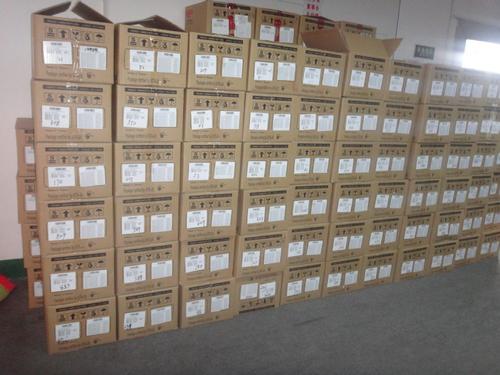
- Solar silicon wafers are typically packaged and shipped in protective containers or trays. These containers are designed to securely hold the wafers in place and protect them from damage during transportation. The wafers are carefully stacked in the packaging with appropriate spacing to prevent any contact or scratching. Additionally, the packaging may include layers of foam or other cushioning materials to provide further protection. Once packaged, the wafers are typically shipped in bulk using suitable shipping methods, such as air freight or specialized carriers, to ensure safe delivery to their destination.
- Q: What is the meaning of a cleaning in a semiconductor silicon wafer process? RCA?
- (4) HPM (SC-2):HCl/H2O2/H2 O from 65 to 85 DEG C is used to remove metal, iron, magnesium and other metal contamination on the surface of silicon wafer. Fe and Zn can be removed by HPM at room temperature.The first is the general idea of cleaning to remove organic contamination on silicon wafer surface, because the organic matter will cover part of the silicon surface, so that the oxide film and related contamination is difficult to remove; then the dissolution of oxide film, the oxide layer is because of "contamination trap", will also introduce epitaxial defects; finally, the removal of particulate and metal contamination, at the same time silicon surface passivation
- Q: How is the wafer appearance caused? The performance of the chip half white, a class of black! Seek help!
- You should be the color difference problem is caused by the mortar temperature cutting room temperature and workshop temperature also influenced to reduce this effect only from the cleaning rod to minimize the time spent between, this is the enthusiasm of the staff problem
- Q: Can solar silicon wafers be used in floating solar power plants?
- Yes, solar silicon wafers can be used in floating solar power plants. These solar wafers, which are made from crystalline silicon, can be integrated into floating photovoltaic (PV) systems to generate electricity from solar energy. Floating solar power plants are becoming increasingly popular due to their ability to maximize land usage and reduce water evaporation.
- Q: Who is the best silicon chip dryer?
- Silicon wafer drying machine is the Wuxi automation technology to do, that is, before the design of the Song Jiang Yang, now is an upgraded version of the. Easy to use.
- Q: What is the typical lead time for ordering solar silicon wafers?
- The typical lead time for ordering solar silicon wafers can vary depending on several factors, including the supplier, quantity, and demand. However, it is common for lead times to range from a few weeks to a few months.
- Q: What is the effect of surface roughness on solar silicon wafers?
- The effect of surface roughness on solar silicon wafers is twofold. Firstly, a rough surface can enhance light trapping, increasing the chances of photon absorption and improving the overall efficiency of the solar cell. Secondly, it can also increase the surface recombination rate of charge carriers, leading to decreased performance. Therefore, a balance must be struck to optimize the surface roughness for maximum solar cell efficiency.
- Q: How are solar silicon wafers protected from hailstorms?
- Solar silicon wafers are typically protected from hailstorms through the use of tempered glass covers or encapsulation materials, which provide a strong barrier against hailstones. Additionally, solar panels are designed and tested to withstand various weather conditions, including hailstorms, ensuring the durability and longevity of the solar cells.
Send your message to us
Silicon Wafer in Solar Photovoltaic Cells - Mono Solar Cells 156mm*156mm in Bulk Quantity Low Price Stock 19.8
- Ref Price:
-
- Loading Port:
- Shanghai
- Payment Terms:
- TT OR LC
- Min Order Qty:
- 1000 pc
- Supply Capability:
- 100000 pc/month
OKorder Service Pledge
OKorder Financial Service
Similar products


Hot products


Hot Searches
Related keywords

