


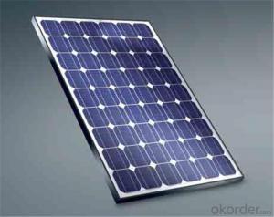
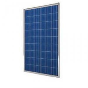
6*6 High Efficiency Mono Silicon Solar Panel Silicon Wafer
- Ref Price:
-

- Loading Port:
- China main port
- Payment Terms:
- TT OR LC
- Min Order Qty:
- 100 watt
- Supply Capability:
- 10000 watt/month
OKorder Service Pledge
OKorder Financial Service
You Might Also Like


Solar Module Summarize
Solar Module is the core part of solar PV power systems,also is the highest value part of it. The function of Solor Module is to convert the sun's radiation to electrical energy, or transfer it to battery and store in it, or to drive the load running.
The Product has been widely used in space and ground, it mainly used for power generation systems, charging systems, road lighting and traffic signs areas. It could offer a wide range of power and voltage, and with high conversion efficiency, and long service life.
Main Characteristic
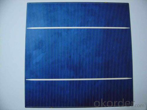
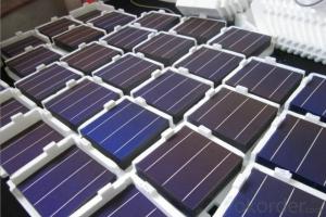
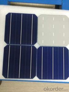
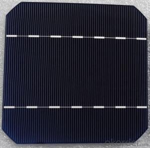
17.6%-18% High Efficiency A Grade 125mm Monocrystalline Solar Cells
1.First-class production technology and packaging technology.
2.Adopting the world's leading technology of silicon and polycrystalline silicon cells, power density, peak hours more battery power, higher conversion efficiency.
3.Beautiful, stable, easy to take down the anodic aluminum frame electric degrees and has a wind-resistant, anti-snow function.
Features
17.6%-18% High Efficiency A Grade 125mm Monocrystalline Solar Cells
1.High transmissivity low-iron tempered glass, strong aluminium frame.
2.Manufactured according to international quality and Environment Management System (ISO9001, ISO14001).
3.Low voltage-temperature coefficient allows higher power output at high-temperature condition.
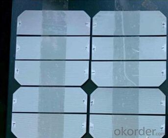
Product Pictures


- Q: How are solar silicon wafers inspected for surface defects?
- Solar silicon wafers are inspected for surface defects using various techniques such as visual inspection, automated optical inspection (AOI), and scanning electron microscopy (SEM). Visual inspection involves examining the wafer surface under proper lighting conditions to identify any visible defects like cracks, scratches, or impurities. AOI utilizes high-resolution cameras and advanced algorithms to scan the wafer surface and detect any abnormalities or inconsistencies. SEM, on the other hand, provides a more detailed analysis by using electron beams to create high-resolution images of the wafer surface, enabling the identification of even smaller defects at a microscopic level. These inspection methods help ensure the quality and efficiency of solar silicon wafers in the production of solar cells.
- Q: What is the cutting fluid for solar wafer cutting?
- MB, HCT, NTC and other machines, the requirements of silicon cutting fluid and the proportion of silicon carbide powder is generally controlled at 1:0.92-0.95, mortar density in 1.630-1.635 can be cut quite ideal. Even if there is a greater proportion of proportion, and even mortar density of 1.67 or so will not have any problems, as long as the mortar viscosity control in 200--250 can be. But Ernst machine for mortar density is not higher than 1.57, that is to say 1.55-1.57. can control the viscosity of mortar at around 150, so the domestic silicon cutting fluid will appear in the 1.57 density with mortar, mortar viscosity may be less than 120, and if the mortar viscosity density to 150, more than 1.57, even more than 1.60. The viscosity of mortar is too large, directly will cause the machine alarm, actually influence deeper and may cause the film does not wash clean, burn, or heating of the motor, bearing on the machine itself is very wear.Therefore, the current domestic solar silicon cutting fluid, it is not very suitable for the Ernst & Young machine. The good news is that domestic users have found the defects of the machine, the machine began to replace the mortar pump from the original 0.75KW into 1.5KW, which may solve this problem.
- Q: In the silicon surface cleaning, there is a final step, the silicon chip into the 4% concentration of HF solution soak for five minutes, to hydrogen passivation treatment, and then rinse with deionized water after nitrogen drying,What is the role and mechanism of this hydrogen passivation?
- Wire cut damage layer thickness of 10 microns.Generally use 20% alkali solution in the corrosion condition at 90 C
- Q: How are solar silicon wafers packaged and shipped?
- Solar silicon wafers are typically packaged and shipped in protective containers or trays. These containers are designed to securely hold the wafers in place and protect them from damage during transportation. The wafers are carefully stacked in the packaging with appropriate spacing to prevent any contact or scratching. Additionally, the packaging may include layers of foam or other cushioning materials to provide further protection. Once packaged, the wafers are typically shipped in bulk using suitable shipping methods, such as air freight or specialized carriers, to ensure safe delivery to their destination.
- Q: How do solar silicon wafers perform in high humidity environments?
- Solar silicon wafers generally perform well in high humidity environments. However, the efficiency of solar panels may slightly decrease due to increased resistance caused by moisture absorption. This can be mitigated by using protective coatings on the surface of the wafers or encapsulating them within moisture-resistant materials. Additionally, regular cleaning and maintenance of the panels can help to maintain optimal performance in high humidity conditions.
- Q: How to make the photoresist and silicon substrate adhesion better
- PR and the same solvent for the HMDS can be better combination, adhesion will be better, will not produce bubble. You can search the TOK OAP material. That's what it's supposed to be
- Q: How are solar silicon wafers packaged for transportation and installation?
- Solar silicon wafers are typically packaged for transportation and installation in protective containers or trays. These containers ensure the wafers are securely stacked and separated to prevent damage during handling and transportation. Additionally, the containers are designed to protect the wafers from moisture, dust, and other contaminants that could affect their performance. Once the wafers reach their destination, they are carefully removed from the packaging and installed in solar modules or panels for use in generating electricity.
- Q: What is the role of texturing in solar silicon wafers?
- The role of texturing in solar silicon wafers is to increase the absorption of sunlight by creating a rough, uneven surface. This texture enhances the amount of light that can be captured by the solar cells, leading to improved energy conversion efficiency.
- Q: How do solar silicon wafers perform in high-altitude environments?
- Solar silicon wafers perform well in high-altitude environments. The thin layer of silicon on the wafers allows for efficient absorption of sunlight, even at higher altitudes where the air is thinner. Additionally, solar panels are designed to withstand various environmental conditions, including temperature changes and exposure to UV radiation. Therefore, solar silicon wafers are suitable for generating electricity in high-altitude areas.
- Q: Can solar silicon wafers be used in space exploration missions?
- Yes, solar silicon wafers can be used in space exploration missions.
Send your message to us
6*6 High Efficiency Mono Silicon Solar Panel Silicon Wafer
- Ref Price:
-
- Loading Port:
- China main port
- Payment Terms:
- TT OR LC
- Min Order Qty:
- 100 watt
- Supply Capability:
- 10000 watt/month
OKorder Service Pledge
OKorder Financial Service
Similar products

Hot products


Hot Searches
Related keywords

