


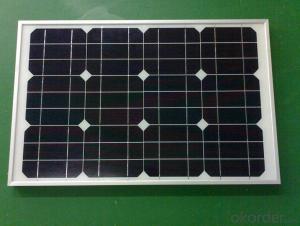
Silicon Wafer for Solar Energy - High Quality A Grade Polycrystalline 5V 16.6% Solar Cell
- Ref Price:
-

- Loading Port:
- Shanghai
- Payment Terms:
- TT OR LC
- Min Order Qty:
- 1000 pc
- Supply Capability:
- 100000 pc/month
OKorder Service Pledge
OKorder Financial Service
You Might Also Like


Specifications
hot sale solar cell
1.16.8%~18.25% high efficiency
2.100% checked quality
3.ISO9001/ISO14001/TUV/CE/UL
4.stable performance
We can offer you the best quality products and services, don't miss !
POLY6'(156*156)
Polycrystalline Silicon Solar cell
Physical Characteristics
Dimension: 156mm×156mm±0.5mm
Diagonal: 220mm±0.5mm
Thickness(Si): 200±20 μm
Front(-) Back(+)
Blue anti-reflecting coating (silicon nitride); Aluminum back surface field;
1.5mm wide bus bars; 2.0mm wide soldering pads;
Distance between bus bars: 51mm . Distance between bus bars :51mm .
Electrical Characteristics
Efficiency(%) | 18.00 | 17.80 | 17.60 | 17.40 | 17.20 | 16.80 | 16.60 | 16.40 | 16.20 | 16.00 | 15.80 | 15.60 |
Pmpp(W) | 4.33 | 4.29 | 4.24 | 4.19 | 4.14 | 4.09 | 4.04 | 3.99 | 3.94 | 3.90 | 3.86 | 3.82 |
Umpp(V) | 0.530 | 0.527 | 0.524 | 0.521 | 0.518 | 0.516 | 0.514 | 0.511 | 0.509 | 0.506 | 0.503 | 0.501 |
Impp(A) | 8.159 | 8.126 | 8.081 | 8.035 | 7.990 | 7.938 | 7.876 | 7.813 | 7.754 | 7.698 | 7.642 | 7.586 |
Uoc(V) | 0.633 | 0.631 | 0.628 | 0.625 | 0.623 | 0.620 | 0.618 | 0.617 | 0.615 | 0.613 | 0.611 | 0.609 |
Isc(A) | 8.709 | 8.677 | 8.629 | 8.578 | 8.531 | 8.478 | 8.419 | 8.356 | 8.289 | 8.220 | 8.151 | 8.083 |

MONO5'(125*125mm)165
Monocrystalline silicon solar cell
Physical Characteristics
Dimension: 125mm×125mm±0.5mm
Diagonal: 165mm±0.5mm
Thickness(Si): 200±20 μm
Front(-) Back(+)
Blue anti-reflecting coating(silicon nitride); Aluminum back surface field;
1.6mmwide bus bars; 2.5mm wide soldering pads;
Distance between bus bars: 61mm . Distance between bus bars :61mm .
Electrical Characteristics
Efficiency(%) | 19.40 | 19.20 | 19.00 | 18.80 | 18.60 | 18.40 | 18.20 | 18.00 | 17.80 | 17.60 | 17.40 | 17.20 |
Pmpp(W) | 2.97 | 2.94 | 2.91 | 2.88 | 2.85 | 2.82 | 2.79 | 2.76 | 2.73 | 2.70 | 2.67 | 2.62 |
Umpp(V) | 0.537 | 0.535 | 0.533 | 0.531 | 0.527 | 0.524 | 0.521 | 0.518 | 0.516 | 0.515 | 0.513 | 0.509 |
Impp(A) | 5.531 | 5.495 | 5.460 | 5.424 | 5.408 | 5.382 | 5.355 | 5.328 | 5.291 | 5.243 | 5.195 | 4.147 |
Uoc(V) | 0.637 | 0.637 | 0.636 | 0.635 | 0.633 | 0.630 | 0.629 | 0.629 | 0.628 | 0.626 | 0.626 | 0.625 |
Isc(A) | 5.888 | 5.876 | 5.862 | 5.848 | 5.839 | 5.826 | 5.809 | 5.791 | 5.779 | 5.756 | 5.293 | 5.144 |

FAQ:
Q:How can i get some sample?
A:Yes , if you want order ,sample is not a problem.
Q:How about your solar panel efficency?
A: Our product efficency around 17.25%~18.25%.
Q:What’s the certificate you have got?
A: we have overall product certificate of ISO9001/ISO14001/CE/TUV/UL
- Q: What is the role of surface passivation on solar silicon wafers?
- The role of surface passivation on solar silicon wafers is to reduce surface recombination and increase the efficiency of the solar cells. Surface passivation helps to minimize the loss of charge carriers at the surface of the silicon wafer, which can significantly improve the overall performance of the solar cells. By creating a protective layer, surface passivation prevents the formation of defects and traps that could hinder the movement of electrons and holes, thus enhancing the conversion of sunlight into electricity.
- Q: How are solar silicon wafers inspected for surface defects?
- Solar silicon wafers are inspected for surface defects using various techniques such as visual inspection, automated optical inspection (AOI), and scanning electron microscopy (SEM). Visual inspection involves examining the wafer surface under proper lighting conditions to identify any visible defects like cracks, scratches, or impurities. AOI utilizes high-resolution cameras and advanced algorithms to scan the wafer surface and detect any abnormalities or inconsistencies. SEM, on the other hand, provides a more detailed analysis by using electron beams to create high-resolution images of the wafer surface, enabling the identification of even smaller defects at a microscopic level. These inspection methods help ensure the quality and efficiency of solar silicon wafers in the production of solar cells.
- Q: How are solar silicon wafers cleaned during the manufacturing process?
- Solar silicon wafers are cleaned during the manufacturing process through a multi-step procedure. Initially, the wafers are subjected to a chemical clean to remove any organic and inorganic impurities present on their surfaces. This involves using acid or alkaline solutions to dissolve and eliminate contaminants. Following the chemical clean, the wafers undergo a rinse process with deionized water to remove any remaining chemicals. Lastly, the wafers are dried using a combination of heat and air or a spin-dry technique to ensure a clean and dry surface before further processing.
- Q: How do solar silicon wafers contribute to the overall cost of a solar panel?
- Solar silicon wafers are a significant contributor to the overall cost of a solar panel. These wafers, which are made from purified silicon, form the base material for manufacturing solar cells. Since silicon is a crucial component for converting sunlight into electricity, the quality and efficiency of the wafers directly impact the panel's performance. The cost of silicon wafers depends on various factors such as purity, size, and production technology. Therefore, any fluctuations in silicon prices can significantly affect the overall cost of a solar panel.
- Q: How do solar silicon wafers perform in coastal areas?
- Solar silicon wafers perform well in coastal areas as they are resistant to corrosion and can withstand the harsh marine environment. The protective layers on the wafers ensure durability against saltwater exposure and high humidity, allowing them to maintain their efficiency and performance over time.
- Q: What is the role of a passivation layer in a solar silicon wafer?
- The role of a passivation layer in a solar silicon wafer is to prevent the recombination of charge carriers at the surface, which improves the efficiency of the solar cell. It acts as a protective coating, reducing surface defects and increasing the overall performance and stability of the solar cell.
- Q: Are solar silicon wafers affected by power grid fluctuations?
- Solar silicon wafers are not directly affected by power grid fluctuations. However, power grid fluctuations can indirectly impact the performance of solar panels, including those with silicon wafers, if the fluctuations result in unstable power supply or voltage variations. In such cases, additional equipment like inverters or voltage regulators might be necessary to ensure the stability and efficiency of solar panel systems.
- Q: Are there any safety concerns associated with handling solar silicon wafers?
- Yes, there are safety concerns associated with handling solar silicon wafers. Silicon wafers are fragile and can easily break, leading to sharp edges that can cause cuts or injuries. Additionally, silicon wafers may emit harmful fumes or dust particles when handled or processed, which can be hazardous if inhaled or ingested. It is important to follow proper handling procedures, wear appropriate protective gear such as gloves and safety glasses, and work in a well-ventilated area to minimize the risks associated with handling solar silicon wafers.
- Q: How do solar silicon wafers affect the aesthetics of buildings?
- Solar silicon wafers have a minimal impact on the aesthetics of buildings. While they are typically dark in color, their installation on rooftops or as building-integrated photovoltaic systems can blend seamlessly with the overall design. Additionally, advancements in solar technology have led to the development of solar panels that can mimic the appearance of traditional roofing materials, further reducing any visual impact on the building's aesthetics.
- Q: How are defects in solar silicon wafers detected?
- Defects in solar silicon wafers are commonly detected through a variety of inspection techniques. One of the primary methods involves visual inspection under bright light or with the help of a microscope to identify any visible cracks, scratches, or impurities on the wafer's surface. Additionally, advanced imaging techniques like infrared thermography, photoluminescence, and electroluminescence can be employed to detect any hidden defects, such as microcracks or material impurities that may not be visible to the naked eye. Electrical tests are also conducted to measure the wafer's electrical properties, including resistivity and carrier lifetime, which can help identify any defects affecting the performance of the solar cell.
Send your message to us
Silicon Wafer for Solar Energy - High Quality A Grade Polycrystalline 5V 16.6% Solar Cell
- Ref Price:
-
- Loading Port:
- Shanghai
- Payment Terms:
- TT OR LC
- Min Order Qty:
- 1000 pc
- Supply Capability:
- 100000 pc/month
OKorder Service Pledge
OKorder Financial Service
Similar products


Hot products


Hot Searches
Related keywords

