


High Current Monocrystalline Solar Silicon Wafer 17.6% Polycrystalline Silicon Solar Cell Price
- Ref Price:
-

- Loading Port:
- Shanghai
- Payment Terms:
- TT OR LC
- Min Order Qty:
- 1000 pc
- Supply Capability:
- 100000 pc/month
OKorder Service Pledge
OKorder Financial Service
You Might Also Like


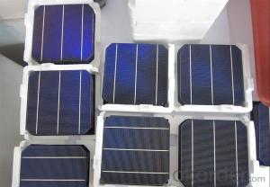
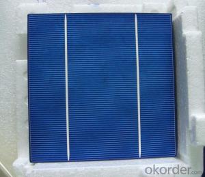
4 Bus Bars 156*156 17.6% efficiency poly solar cell
PHYSICAL CHARACTERISTICS
Dimension: 156mm x 156mm ± 0.5mm
Wafer Thickeness: 180um+20um and 200um+20um
Front(-) Four 1.2mm silver busbar
Silicon nitride blue anti-reflection coating
Back(+) aluminum back surface field
1.75mm(silver) wide segment soldering pads

Typical Electrical Characteristics
Efficiency | W(Pmpp) | V(Umpp) | A(Impp) | V(Uoc) | A(Isc) |
17.4-17.5 | 4.234 | 0.517 | 8.231 | 0.622 | 8.759 |
17.5-17.6 | 4.259 | 0.519 | 8.243 | 0.623 | 8.769 |
17.7-17.8 | 4.283 | 0.521 | 8.256 | 0.625 | 8.779 |
17.8-17.9 | 4.307 | 0.523 | 8.268 | 0.626 | 8.788 |
17.9-18.0 | 4.332 | 0.525 | 8.281 | 0.627 | 8.798 |
18.0-18.1 | 4.380 | 0.529 | 8.306 | 0.629 | 8.808 |
18.1-18.2 | 4.405 | 0.531 | 8.318 | 0.632 | 8.818 |
18.2-18.3 | 4.429 | 0.533 | 8.331 | 0.633 | 8.837 |
18.3-18.4 | 4.453 | 0.535 | 8.344 | 0.634 | 8.847 |
18.4-18.5 | 4.478 | 0.537 | 8.356 | 0.636 | 8.856 |
18.5-18.6 | 4.502 | 0.539 | 8.369 | 0.637 | 8.866 |
Efficiency | W(Pmpp) | V(Umpp) | A(Impp) | V(Uoc) | A(Isc) |
20.90-21.00 | 5.06 | 0.557 | 9.007 | 0.653 | 9.688 |
20.80-20.90 | 5.04 | 0.556 | 9.062 | 0.652 | 9.683 |
20.70-20.80 | 5.02 | 0.554 | 9.055 | 0.651 | 9.684 |
20.60-20.70 | 4.99 | 0.552 | 9.033 | 0.651 | 9.672 |
20.50-20.60 | 4.97 | 0.550 | 9.002 | 0.650 | 9.673 |
20.40-20.50 | 4.94 | 0.548 | 9.012 | 0.649 | 9.674 |
20.30-20.40 | 4.92 | 0.546 | 9.009 | 0.649 | 9.655 |
20.20-20.30 | 4.89 | 0.543 | 9.012 | 0.648 | 9.634 |
20.10-20.20 | 4.87 | 0.541 | 8.998 | 0.648 | 9.617 |
20.00-20.10 | 4.85 | 0.540 | 8.977 | 0.647 | 9.600 |
*Data under standard testing conditional (STC):1,000w/m2,AM1.5, 25°C , Pmax:Positive power tolerance.
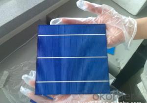
3 Bus Bars 156*156 17.4% efficiency poly solar cell
Dimension: 156 mm x 156 mm ± 0.5 mm
Wafer Thickeness: 156 mm x 156 mm ± 0.5 mm

Typical Electrical Characteristics:
| Efficiency code | 1660 | 1680 | 1700 | 1720 | 1740 | 1760 | 1780 | 1800 | 1820 | 1840 | 1860 |
| Efficiency (%) | 16.6 | 16.8 | 17.0 | 17.2 | 17.4 | 17.6 | 17.8 | 18.0 | 18.2 | 18.4 | 18.6 |
| Pmax (W) | 4.04 | 4.09 | 4.14 | 4.19 | 4.23 | 4.28 | 4.33 | 4.38 | 4.43 | 4.48 | 4.53 |
| Voc (V) | 0.612 | 0.615 | 0.618 | 0.621 | 0.624 | 0.627 | 0.629 | 0.63 | 0.633 | 0.635 | 0.637 |
| Isc (A) | 8.42 | 8.46 | 8.51 | 8.56 | 8.61 | 8.65 | 8.69 | 8.73 | 8.77 | 8.81 | 8.84 |
| Imp (A) | 7.91 | 7.99 | 8.08 | 8.16 | 8.22 | 8.27 | 8.33 | 8.38 | 8.43 | 8.48 | 8.53 |
* Testing conditions: 1000 W/m2, AM 1.5, 25 °C, Tolerance: Efficiency ± 0.2% abs., Pmpp ±1.5% rel.
* Imin : at 0.5 V
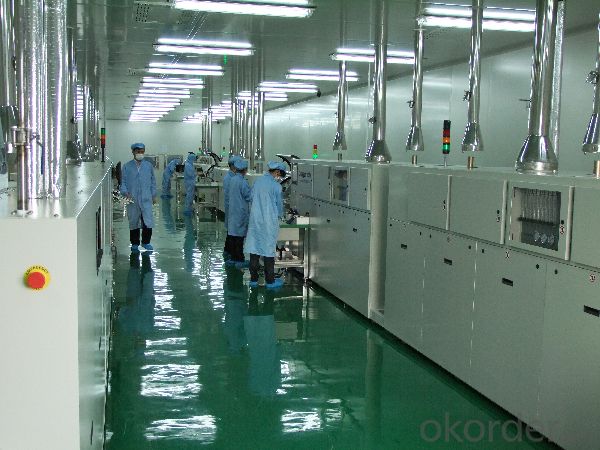
Production:

Package:

FAQ:
1. Q: Do you have your own factory?
A: Yes, we have. Our factory located in Jiangsu
2. Q: How can I visit your factory?
A: Before you visit,please contact us.We will show you the route or arrange a car to pick you up.
3. Q: Do you provide free sample?
A: Commenly we provide paid sample.
4. Q: Could you print our company LOGO on the nameplate and package?
A: Yes, we accept it.And need an Authorization Letter from you.
5. Q: Do you accept custom design on size?
A: Yes, if the size is reasonable.
6. Q: How can I be your agent in my country?
A: Please leave feedback. It's better for us to talk about details by email.
7. Q: Do you have solar project engineer who can guide me to install system?
A: Yes, we have a professional engineer team. They can teach you how to install a solar system.
- Q: What is the typical warranty period for a solar silicon wafer?
- The typical warranty period for a solar silicon wafer is around 25 to 30 years.
- Q: What is the impact of impurities in solar silicon wafers on performance?
- Impurities in solar silicon wafers can have a significant impact on the performance of solar cells. These impurities, such as metal contaminants or dopants, can introduce defects in the crystal structure of the silicon, affecting the efficiency of electron movement and trapping photons. This can lead to reduced power output, decreased conversion efficiency, and shorter lifespan of the solar cells. Therefore, it is crucial to minimize impurities during the manufacturing process to optimize the performance and overall quality of solar silicon wafers.
- Q: What are the impurities in a solar silicon wafer?
- The impurities commonly found in a solar silicon wafer include dopants such as boron or phosphorus, which are intentionally introduced to create the desired electrical properties. Other impurities can include metallic contaminants like iron, aluminum, or copper, which can negatively affect the performance of the solar cell.
- Q: What is the purpose of surface texturing in solar silicon wafers?
- The purpose of surface texturing in solar silicon wafers is to increase the light absorption capability of the wafer by creating microstructures on its surface. These microstructures help to trap and scatter light, allowing for more efficient capture of sunlight and conversion into electricity.
- Q: What is the purpose of texturing the surface of a solar silicon wafer?
- The purpose of texturing the surface of a solar silicon wafer is to increase its light absorption capacity. By introducing microscopic structures or patterns on the wafer's surface, the texture helps to scatter and trap light, allowing for better interaction with the silicon material and enhancing the overall efficiency of the solar cell.
- Q: What is the typical weight of a solar silicon wafer?
- The typical weight of a solar silicon wafer is around 2 to 4 grams.
- Q: After cutting a few chips, mortar density is getting lower and lower
- PEG water absorption is very strong, as long as the air humidity is slightly higher, then did not cut the water content of a mortar on the rise, as well as the viscosity of mortar and mortar temperature is related to the temperature difference, the viscosity of mortar to a difference of about 10
- Q: What is the expected efficiency improvement for tandem perovskite-silicon solar silicon wafers?
- The expected efficiency improvement for tandem perovskite-silicon solar silicon wafers is significant, with the potential to surpass the efficiency of traditional silicon solar cells. Tandem perovskite-silicon solar cells combine the unique properties of perovskite materials with high-performance silicon cells, allowing for improved light absorption and conversion of solar energy into electricity. This technology has already demonstrated promising efficiency improvements in lab settings, and with further advancements and optimization, it holds great potential for enhancing the overall efficiency of solar power generation.
- Q: How are solar silicon wafers etched to enhance light absorption?
- Solar silicon wafers are etched to enhance light absorption through a process called texturization. This involves using an etching solution, such as a mixture of hydrofluoric acid and nitric acid, to etch the surface of the silicon wafer. The etching solution removes small amounts of silicon, creating microscopic pyramids or bumps on the surface. These surface textures help trap and scatter incoming light, increasing the chances of absorption by the silicon material and improving the overall efficiency of the solar cell.
- Q: How do solar silicon wafers perform in low light conditions?
- Solar silicon wafers perform relatively well in low light conditions compared to other solar technologies. Although their efficiency decreases, they can still generate electricity due to their ability to convert even small amounts of sunlight into energy. However, their performance is significantly reduced during overcast skies or in shaded areas where access to direct sunlight is limited.
Send your message to us
High Current Monocrystalline Solar Silicon Wafer 17.6% Polycrystalline Silicon Solar Cell Price
- Ref Price:
-
- Loading Port:
- Shanghai
- Payment Terms:
- TT OR LC
- Min Order Qty:
- 1000 pc
- Supply Capability:
- 100000 pc/month
OKorder Service Pledge
OKorder Financial Service
Similar products


Hot products


Hot Searches
Related keywords

