


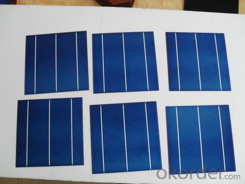


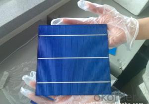
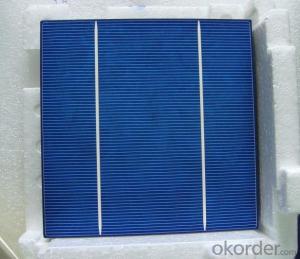
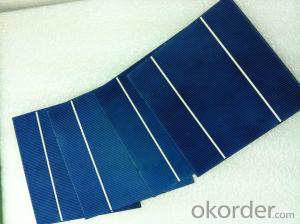
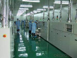
Jinko Solar Silicon Wafer High Current 17.0% Polycrystalline Silicon Solar Cell
- Ref Price:
-

- Loading Port:
- Shanghai
- Payment Terms:
- TT OR LC
- Min Order Qty:
- 1000 pc
- Supply Capability:
- 100000 pc/month
OKorder Service Pledge
OKorder Financial Service
You Might Also Like


4 Bus Bars 156*156 17.6% efficiency poly solar cell
PHYSICAL CHARACTERISTICS
Dimension: 156mm x 156mm ± 0.5mm
Wafer Thickeness: 180um+20um and 200um+20um
Front(-) Four 1.2mm silver busbar
Silicon nitride blue anti-reflection coating
Back(+) aluminum back surface field
1.75mm(silver) wide segment soldering pads

Typical Electrical Characteristics
Efficiency | W(Pmpp) | V(Umpp) | A(Impp) | V(Uoc) | A(Isc) |
17.4-17.5 | 4.234 | 0.517 | 8.231 | 0.622 | 8.759 |
17.5-17.6 | 4.259 | 0.519 | 8.243 | 0.623 | 8.769 |
17.7-17.8 | 4.283 | 0.521 | 8.256 | 0.625 | 8.779 |
17.8-17.9 | 4.307 | 0.523 | 8.268 | 0.626 | 8.788 |
17.9-18.0 | 4.332 | 0.525 | 8.281 | 0.627 | 8.798 |
18.0-18.1 | 4.380 | 0.529 | 8.306 | 0.629 | 8.808 |
18.1-18.2 | 4.405 | 0.531 | 8.318 | 0.632 | 8.818 |
18.2-18.3 | 4.429 | 0.533 | 8.331 | 0.633 | 8.837 |
18.3-18.4 | 4.453 | 0.535 | 8.344 | 0.634 | 8.847 |
18.4-18.5 | 4.478 | 0.537 | 8.356 | 0.636 | 8.856 |
18.5-18.6 | 4.502 | 0.539 | 8.369 | 0.637 | 8.866 |
Efficiency | W(Pmpp) | V(Umpp) | A(Impp) | V(Uoc) | A(Isc) |
20.90-21.00 | 5.06 | 0.557 | 9.007 | 0.653 | 9.688 |
20.80-20.90 | 5.04 | 0.556 | 9.062 | 0.652 | 9.683 |
20.70-20.80 | 5.02 | 0.554 | 9.055 | 0.651 | 9.684 |
20.60-20.70 | 4.99 | 0.552 | 9.033 | 0.651 | 9.672 |
20.50-20.60 | 4.97 | 0.550 | 9.002 | 0.650 | 9.673 |
20.40-20.50 | 4.94 | 0.548 | 9.012 | 0.649 | 9.674 |
20.30-20.40 | 4.92 | 0.546 | 9.009 | 0.649 | 9.655 |
20.20-20.30 | 4.89 | 0.543 | 9.012 | 0.648 | 9.634 |
20.10-20.20 | 4.87 | 0.541 | 8.998 | 0.648 | 9.617 |
20.00-20.10 | 4.85 | 0.540 | 8.977 | 0.647 | 9.600 |
*Data under standard testing conditional (STC):1,000w/m2,AM1.5, 25°C , Pmax:Positive power tolerance.
3 Bus Bars 156*156 17.4% efficiency poly solar cell
Dimension: 156 mm x 156 mm ± 0.5 mm
Wafer Thickeness: 156 mm x 156 mm ± 0.5 mm

Typical Electrical Characteristics:
| Efficiency code | 1660 | 1680 | 1700 | 1720 | 1740 | 1760 | 1780 | 1800 | 1820 | 1840 | 1860 |
| Efficiency (%) | 16.6 | 16.8 | 17.0 | 17.2 | 17.4 | 17.6 | 17.8 | 18.0 | 18.2 | 18.4 | 18.6 |
| Pmax (W) | 4.04 | 4.09 | 4.14 | 4.19 | 4.23 | 4.28 | 4.33 | 4.38 | 4.43 | 4.48 | 4.53 |
| Voc (V) | 0.612 | 0.615 | 0.618 | 0.621 | 0.624 | 0.627 | 0.629 | 0.63 | 0.633 | 0.635 | 0.637 |
| Isc (A) | 8.42 | 8.46 | 8.51 | 8.56 | 8.61 | 8.65 | 8.69 | 8.73 | 8.77 | 8.81 | 8.84 |
| Imp (A) | 7.91 | 7.99 | 8.08 | 8.16 | 8.22 | 8.27 | 8.33 | 8.38 | 8.43 | 8.48 | 8.53 |
* Testing conditions: 1000 W/m2, AM 1.5, 25 °C, Tolerance: Efficiency ± 0.2% abs., Pmpp ±1.5% rel.
* Imin : at 0.5 V
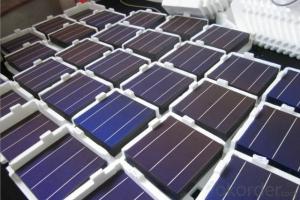
Production:

Package:

FAQ:
1. Q: Do you have your own factory?
A: Yes, we have. Our factory located in Jiangsu
2. Q: How can I visit your factory?
A: Before you visit,please contact us.We will show you the route or arrange a car to pick you up.
3. Q: Do you provide free sample?
A: Commenly we provide paid sample.
4. Q: Could you print our company LOGO on the nameplate and package?
A: Yes, we accept it.And need an Authorization Letter from you.
5. Q: Do you accept custom design on size?
A: Yes, if the size is reasonable.
6. Q: How can I be your agent in my country?
A: Please leave feedback. It's better for us to talk about details by email.
7. Q: Do you have solar project engineer who can guide me to install system?
A: Yes, we have a professional engineer team. They can teach you how to install a solar system.
- Q: What is the role of surface passivation on solar silicon wafers?
- The role of surface passivation on solar silicon wafers is to improve the efficiency and performance of the solar cells. Passivation involves the application of a thin layer of material on the surface of the silicon wafer to reduce surface recombination, which is the loss of electrons and holes at the surface. This helps to minimize the loss of charge carriers and improves the overall electrical properties of the solar cell. By reducing surface recombination, surface passivation increases the conversion efficiency of the solar cell and enhances its ability to generate electricity from sunlight.
- Q: What is the effect of temperature on the efficiency of a solar silicon wafer?
- The temperature has a significant effect on the efficiency of a solar silicon wafer. As the temperature increases, the efficiency of the wafer decreases. This is because higher temperatures can lead to increased resistance in the wafer, which in turn reduces the flow of electricity. Additionally, higher temperatures can cause the semiconductor properties of the wafer to degrade, resulting in a decrease in its ability to convert sunlight into electricity. Therefore, controlling and minimizing the temperature of the solar silicon wafer is crucial for maximizing its efficiency and overall performance.
- Q: How do solar silicon wafers perform in high wind conditions?
- Solar silicon wafers can generally withstand high wind conditions without significant impact on performance. However, extreme wind speeds can cause minor vibrations or deflections in the panels, potentially affecting their efficiency. To mitigate this, solar installations are designed to withstand standard wind speeds and are often equipped with secure mounting systems.
- Q: What is the efficiency of a solar silicon wafer?
- The efficiency of a solar silicon wafer refers to its ability to convert sunlight into electricity. It is typically measured as a percentage of the incoming sunlight that is successfully converted into usable electrical energy. The efficiency can vary depending on various factors including the quality and composition of the silicon wafer, the manufacturing process, and the environmental conditions. Generally, the efficiency of a solar silicon wafer ranges from around 15% to 25%, with higher quality and more advanced technologies achieving higher efficiencies.
- Q: Are solar silicon wafers affected by humidity?
- Yes, solar silicon wafers can be affected by humidity. High humidity levels can impact the performance and efficiency of solar cells made from silicon wafers. Moisture can cause corrosion, reduce electrical conductivity, and potentially damage the surface of the wafers. Therefore, it is important to protect solar silicon wafers from excessive humidity to ensure optimal functionality and longevity.
- Q: What are the different doping techniques used in solar silicon wafers?
- There are several doping techniques used in solar silicon wafers, including diffusion, ion implantation, and screen-printing. Diffusion involves introducing dopant atoms, such as phosphorus or boron, into the silicon wafer by heating it in the presence of a dopant source. Ion implantation involves bombarding the wafer with dopant ions, which then become embedded in the silicon lattice. Screen-printing involves applying a dopant paste onto the surface of the wafer and then firing it to create a doped layer. These techniques are used to create the necessary p-n junctions and optimize the electrical properties of the solar cells.
- Q: What is the price of monocrystalline silicon
- The current price of silicon wafer recycling depends on the quality of the silicon wafer.
- Q: What is the role of solar silicon wafers in the overall solar energy system?
- Solar silicon wafers play a crucial role in the overall solar energy system as they are the key component in photovoltaic (PV) cells, which convert sunlight into electricity. These wafers, made from high-purity silicon, are responsible for absorbing sunlight and generating a flow of electrons, thus producing direct current (DC) electricity. They are the foundation of solar panels and are essential for harnessing solar energy on a large scale.
- Q: The significance of silicon wafer heat treatment
- 2, heat treatment of several temperature interval concept:Thermal donor: 350-550 degrees Celsius, 450 degrees Celsius450 C after heat treatment (or equivalent effect, such as the cooling of a single crystal in a furnace), the resistivity of the N type sample can be decreased and the resistivity of the P type sample is increased, as is the introduction of a certain number of donor phenomena. This is due to the temperature of the dissolved oxygen atoms in the formation of complex (SiO4) caused by the thermal donor, the resistivity of silicon and oxygen content of the four side is inversely proportional to.New donor: 550-800 DEG C, on behalf of the temperature of 650 degrees Celsius
- Q: Are there any government regulations or standards for solar silicon wafers?
- Yes, there are government regulations and standards for solar silicon wafers. These regulations and standards vary from country to country and are implemented to ensure the quality, efficiency, and safety of solar silicon wafers used in photovoltaic systems. They typically cover aspects such as material composition, purity levels, dimensions, electrical performance, and environmental impact. Compliance with these regulations and standards is essential for manufacturers and suppliers to meet industry requirements and ensure the reliability and performance of solar energy systems.
Send your message to us
Jinko Solar Silicon Wafer High Current 17.0% Polycrystalline Silicon Solar Cell
- Ref Price:
-
- Loading Port:
- Shanghai
- Payment Terms:
- TT OR LC
- Min Order Qty:
- 1000 pc
- Supply Capability:
- 100000 pc/month
OKorder Service Pledge
OKorder Financial Service
Similar products

Hot products


Hot Searches
Related keywords

