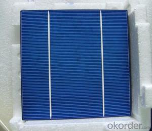
High Current Solar Cell 18.2% Polycrystalline Silicon Solar Cell Price
- Ref Price:
-

- Loading Port:
- Shanghai
- Payment Terms:
- TT OR LC
- Min Order Qty:
- 1000 pc
- Supply Capability:
- 100000 pc/month
OKorder Service Pledge
OKorder Financial Service
You Might Also Like


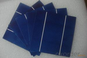
4 Bus Bars 156*156 17.6% efficiency poly solar cell
PHYSICAL CHARACTERISTICS
Dimension: 156mm x 156mm ± 0.5mm
Wafer Thickeness: 180um+20um and 200um+20um
Front(-) Four 1.2mm silver busbar
Silicon nitride blue anti-reflection coating
Back(+) aluminum back surface field
1.75mm(silver) wide segment soldering pads

Typical Electrical Characteristics
Efficiency | W(Pmpp) | V(Umpp) | A(Impp) | V(Uoc) | A(Isc) |
17.4-17.5 | 4.234 | 0.517 | 8.231 | 0.622 | 8.759 |
17.5-17.6 | 4.259 | 0.519 | 8.243 | 0.623 | 8.769 |
17.7-17.8 | 4.283 | 0.521 | 8.256 | 0.625 | 8.779 |
17.8-17.9 | 4.307 | 0.523 | 8.268 | 0.626 | 8.788 |
17.9-18.0 | 4.332 | 0.525 | 8.281 | 0.627 | 8.798 |
18.0-18.1 | 4.380 | 0.529 | 8.306 | 0.629 | 8.808 |
18.1-18.2 | 4.405 | 0.531 | 8.318 | 0.632 | 8.818 |
18.2-18.3 | 4.429 | 0.533 | 8.331 | 0.633 | 8.837 |
18.3-18.4 | 4.453 | 0.535 | 8.344 | 0.634 | 8.847 |
18.4-18.5 | 4.478 | 0.537 | 8.356 | 0.636 | 8.856 |
18.5-18.6 | 4.502 | 0.539 | 8.369 | 0.637 | 8.866 |
Efficiency | W(Pmpp) | V(Umpp) | A(Impp) | V(Uoc) | A(Isc) |
20.90-21.00 | 5.06 | 0.557 | 9.007 | 0.653 | 9.688 |
20.80-20.90 | 5.04 | 0.556 | 9.062 | 0.652 | 9.683 |
20.70-20.80 | 5.02 | 0.554 | 9.055 | 0.651 | 9.684 |
20.60-20.70 | 4.99 | 0.552 | 9.033 | 0.651 | 9.672 |
20.50-20.60 | 4.97 | 0.550 | 9.002 | 0.650 | 9.673 |
20.40-20.50 | 4.94 | 0.548 | 9.012 | 0.649 | 9.674 |
20.30-20.40 | 4.92 | 0.546 | 9.009 | 0.649 | 9.655 |
20.20-20.30 | 4.89 | 0.543 | 9.012 | 0.648 | 9.634 |
20.10-20.20 | 4.87 | 0.541 | 8.998 | 0.648 | 9.617 |
20.00-20.10 | 4.85 | 0.540 | 8.977 | 0.647 | 9.600 |
*Data under standard testing conditional (STC):1,000w/m2,AM1.5, 25°C , Pmax:Positive power tolerance.
3 Bus Bars 156*156 17.4% efficiency poly solar cell
Dimension: 156 mm x 156 mm ± 0.5 mm
Wafer Thickeness: 156 mm x 156 mm ± 0.5 mm

Typical Electrical Characteristics:
| Efficiency code | 1660 | 1680 | 1700 | 1720 | 1740 | 1760 | 1780 | 1800 | 1820 | 1840 | 1860 |
| Efficiency (%) | 16.6 | 16.8 | 17.0 | 17.2 | 17.4 | 17.6 | 17.8 | 18.0 | 18.2 | 18.4 | 18.6 |
| Pmax (W) | 4.04 | 4.09 | 4.14 | 4.19 | 4.23 | 4.28 | 4.33 | 4.38 | 4.43 | 4.48 | 4.53 |
| Voc (V) | 0.612 | 0.615 | 0.618 | 0.621 | 0.624 | 0.627 | 0.629 | 0.63 | 0.633 | 0.635 | 0.637 |
| Isc (A) | 8.42 | 8.46 | 8.51 | 8.56 | 8.61 | 8.65 | 8.69 | 8.73 | 8.77 | 8.81 | 8.84 |
| Imp (A) | 7.91 | 7.99 | 8.08 | 8.16 | 8.22 | 8.27 | 8.33 | 8.38 | 8.43 | 8.48 | 8.53 |
* Testing conditions: 1000 W/m2, AM 1.5, 25 °C, Tolerance: Efficiency ± 0.2% abs., Pmpp ±1.5% rel.
* Imin : at 0.5 V
Production:

Package:

FAQ:
1. Q: Do you have your own factory?
A: Yes, we have. Our factory located in Jiangsu
2. Q: How can I visit your factory?
A: Before you visit,please contact us.We will show you the route or arrange a car to pick you up.
3. Q: Do you provide free sample?
A: Commenly we provide paid sample.
4. Q: Could you print our company LOGO on the nameplate and package?
A: Yes, we accept it.And need an Authorization Letter from you.
5. Q: Do you accept custom design on size?
A: Yes, if the size is reasonable.
6. Q: How can I be your agent in my country?
A: Please leave feedback. It's better for us to talk about details by email.
7. Q: Do you have solar project engineer who can guide me to install system?
A: Yes, we have a professional engineer team. They can teach you how to install a solar system.
- Q:How is a frame attached to a solar silicon wafer?
- A frame is typically attached to a solar silicon wafer using a combination of adhesive materials and mechanical fasteners. The wafer is first secured onto a backing material, such as a glass or plastic sheet, and then the frame is placed around the wafer. Adhesive materials, such as epoxy or silicone, are applied to bond the frame to the wafer and ensure a secure attachment. Additionally, mechanical fasteners like screws or clips may be used to further reinforce the connection between the frame and the wafer. This combined approach provides stability and protection to the solar silicon wafer during installation and operation.
- Q:The higher the resistivity of silicon wafers, the better?!!! 1 experts please answer me!
- Low resistivity is helpful to improve the opening pressure, high resistivity and help to improve the short-circuit current, the best match between the two is about 1 -3! Own understanding!
- Q:How does the thickness of a passivation layer affect the efficiency of a solar silicon wafer?
- The thickness of a passivation layer on a solar silicon wafer directly impacts its efficiency. A thicker passivation layer can enhance the effectiveness of surface passivation, reducing surface recombination and improving the overall efficiency of the solar cell. However, if the passivation layer becomes too thick, it may introduce additional defects or hinder the diffusion of charge carriers, leading to a decrease in efficiency. Therefore, an optimal thickness of the passivation layer needs to be carefully determined to maximize the efficiency of the solar silicon wafer.
- Q:I would like to ask what the purpose of the use of semiconductor silicon wafers, doped with boron ah?
- PN junction has a single conductivity, semiconductor rectifier is made of the characteristics of the PN junction. Such as: large scale integrated circuit is under the high temperature for the impurity required in a certain way (thermal diffusion and ion implantation) incorporated into the silicon wafer surface layer, and make it reach the required quantity and distribution, manufacturing a PN junction, interconnect and ohmic contact to complete.
- Q:Can solar silicon wafers be used in desert regions?
- Yes, solar silicon wafers can be used in desert regions. In fact, desert regions are ideal for solar energy generation due to their abundant sunlight and high solar irradiance. The dry and arid climate in deserts also helps to maintain the efficiency of solar panels by reducing the moisture and dust accumulation on the surface of the silicon wafers.
- Q:Can solar silicon wafers be used in remote off-grid locations?
- Yes, solar silicon wafers can be used in remote off-grid locations. Solar panels made from silicon wafers are commonly used to generate electricity in areas without access to a traditional power grid. These panels are designed to capture sunlight and convert it into usable energy, making them suitable for off-grid locations where they can provide a reliable and renewable source of power.
- Q:How does the efficiency of a solar silicon wafer change with time of day?
- The efficiency of a solar silicon wafer typically fluctuates with the time of day. It tends to be highest during peak sunlight hours, which are typically around midday, and decreases as the sun moves closer to sunrise or sunset. This is because the intensity of sunlight is strongest when the sun is directly overhead, providing maximum energy for the solar panel to convert into electricity. As the angle of the sun changes throughout the day, the amount of sunlight reaching the solar wafer reduces, resulting in a decrease in efficiency.
- Q:What is the purpose of a temperature coefficient in a solar silicon wafer?
- The purpose of a temperature coefficient in a solar silicon wafer is to quantify how the performance and efficiency of the solar cell are affected by changes in temperature. It allows us to understand and account for the variations in electrical output that occur as the temperature of the solar cell changes, helping in the accurate prediction and optimization of solar cell performance under different temperature conditions.
- Q:How is a grounding wire connected to a solar silicon wafer?
- A grounding wire is typically connected to a solar silicon wafer by attaching it to the metal frame or the backside of the wafer using a conductive adhesive or a soldering process.
- Q:What factors affect the conversion efficiency of a solar silicon wafer?
- Several factors affect the conversion efficiency of a solar silicon wafer. Firstly, the quality and purity of the silicon material used in the wafer play a crucial role. Higher purity levels result in lower energy losses and better conversion efficiency. Additionally, the thickness and surface texture of the silicon wafer can impact the efficiency. Thinner wafers allow for better light absorption, while textured surfaces enhance light trapping. The design and positioning of the solar cells on the wafer, as well as the type and quality of the anti-reflective coating used, also influence the conversion efficiency. Furthermore, external factors such as temperature, sunlight intensity, and shading can impact conversion efficiency. Overall, optimizing these factors is essential to maximize the energy conversion efficiency of a solar silicon wafer.
1. Manufacturer Overview |
|
|---|---|
| Location | |
| Year Established | |
| Annual Output Value | |
| Main Markets | |
| Company Certifications | |
2. Manufacturer Certificates |
|
|---|---|
| a) Certification Name | |
| Range | |
| Reference | |
| Validity Period | |
3. Manufacturer Capability |
|
|---|---|
| a)Trade Capacity | |
| Nearest Port | |
| Export Percentage | |
| No.of Employees in Trade Department | |
| Language Spoken: | |
| b)Factory Information | |
| Factory Size: | |
| No. of Production Lines | |
| Contract Manufacturing | |
| Product Price Range | |
Send your message to us
High Current Solar Cell 18.2% Polycrystalline Silicon Solar Cell Price
- Ref Price:
-
- Loading Port:
- Shanghai
- Payment Terms:
- TT OR LC
- Min Order Qty:
- 1000 pc
- Supply Capability:
- 100000 pc/month
OKorder Service Pledge
OKorder Financial Service
Similar products


New products

Hot products


Hot Searches
Related keywords