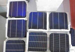


High Current Solar Cell 16.8% Polycrystalline Silicon Solar Cell Price
- Ref Price:
-

- Loading Port:
- Shanghai
- Payment Terms:
- TT OR LC
- Min Order Qty:
- 1000 pc
- Supply Capability:
- 100000 pc/month
OKorder Service Pledge
OKorder Financial Service
You Might Also Like


4 Bus Bars 156*156 17.6% efficiency poly solar cell
PHYSICAL CHARACTERISTICS
Dimension: 156mm x 156mm ± 0.5mm
Wafer Thickeness: 180um+20um and 200um+20um
Front(-) Four 1.2mm silver busbar
Silicon nitride blue anti-reflection coating
Back(+) aluminum back surface field
1.75mm(silver) wide segment soldering pads

Typical Electrical Characteristics
Efficiency | W(Pmpp) | V(Umpp) | A(Impp) | V(Uoc) | A(Isc) |
17.4-17.5 | 4.234 | 0.517 | 8.231 | 0.622 | 8.759 |
17.5-17.6 | 4.259 | 0.519 | 8.243 | 0.623 | 8.769 |
17.7-17.8 | 4.283 | 0.521 | 8.256 | 0.625 | 8.779 |
17.8-17.9 | 4.307 | 0.523 | 8.268 | 0.626 | 8.788 |
17.9-18.0 | 4.332 | 0.525 | 8.281 | 0.627 | 8.798 |
18.0-18.1 | 4.380 | 0.529 | 8.306 | 0.629 | 8.808 |
18.1-18.2 | 4.405 | 0.531 | 8.318 | 0.632 | 8.818 |
18.2-18.3 | 4.429 | 0.533 | 8.331 | 0.633 | 8.837 |
18.3-18.4 | 4.453 | 0.535 | 8.344 | 0.634 | 8.847 |
18.4-18.5 | 4.478 | 0.537 | 8.356 | 0.636 | 8.856 |
18.5-18.6 | 4.502 | 0.539 | 8.369 | 0.637 | 8.866 |
Efficiency | W(Pmpp) | V(Umpp) | A(Impp) | V(Uoc) | A(Isc) |
20.90-21.00 | 5.06 | 0.557 | 9.007 | 0.653 | 9.688 |
20.80-20.90 | 5.04 | 0.556 | 9.062 | 0.652 | 9.683 |
20.70-20.80 | 5.02 | 0.554 | 9.055 | 0.651 | 9.684 |
20.60-20.70 | 4.99 | 0.552 | 9.033 | 0.651 | 9.672 |
20.50-20.60 | 4.97 | 0.550 | 9.002 | 0.650 | 9.673 |
20.40-20.50 | 4.94 | 0.548 | 9.012 | 0.649 | 9.674 |
20.30-20.40 | 4.92 | 0.546 | 9.009 | 0.649 | 9.655 |
20.20-20.30 | 4.89 | 0.543 | 9.012 | 0.648 | 9.634 |
20.10-20.20 | 4.87 | 0.541 | 8.998 | 0.648 | 9.617 |
20.00-20.10 | 4.85 | 0.540 | 8.977 | 0.647 | 9.600 |
*Data under standard testing conditional (STC):1,000w/m2,AM1.5, 25°C , Pmax:Positive power tolerance.
3 Bus Bars 156*156 17.4% efficiency poly solar cell
Dimension: 156 mm x 156 mm ± 0.5 mm
Wafer Thickeness: 156 mm x 156 mm ± 0.5 mm

Typical Electrical Characteristics:
| Efficiency code | 1660 | 1680 | 1700 | 1720 | 1740 | 1760 | 1780 | 1800 | 1820 | 1840 | 1860 |
| Efficiency (%) | 16.6 | 16.8 | 17.0 | 17.2 | 17.4 | 17.6 | 17.8 | 18.0 | 18.2 | 18.4 | 18.6 |
| Pmax (W) | 4.04 | 4.09 | 4.14 | 4.19 | 4.23 | 4.28 | 4.33 | 4.38 | 4.43 | 4.48 | 4.53 |
| Voc (V) | 0.612 | 0.615 | 0.618 | 0.621 | 0.624 | 0.627 | 0.629 | 0.63 | 0.633 | 0.635 | 0.637 |
| Isc (A) | 8.42 | 8.46 | 8.51 | 8.56 | 8.61 | 8.65 | 8.69 | 8.73 | 8.77 | 8.81 | 8.84 |
| Imp (A) | 7.91 | 7.99 | 8.08 | 8.16 | 8.22 | 8.27 | 8.33 | 8.38 | 8.43 | 8.48 | 8.53 |
* Testing conditions: 1000 W/m2, AM 1.5, 25 °C, Tolerance: Efficiency ± 0.2% abs., Pmpp ±1.5% rel.
* Imin : at 0.5 V
Production:

Package:

FAQ:
1. Q: Do you have your own factory?
A: Yes, we have. Our factory located in Jiangsu
2. Q: How can I visit your factory?
A: Before you visit,please contact us.We will show you the route or arrange a car to pick you up.
3. Q: Do you provide free sample?
A: Commenly we provide paid sample.
4. Q: Could you print our company LOGO on the nameplate and package?
A: Yes, we accept it.And need an Authorization Letter from you.
5. Q: Do you accept custom design on size?
A: Yes, if the size is reasonable.
6. Q: How can I be your agent in my country?
A: Please leave feedback. It's better for us to talk about details by email.
7. Q: Do you have solar project engineer who can guide me to install system?
A: Yes, we have a professional engineer team. They can teach you how to install a solar system.
- Q:Is a wafer a silicon wafer and a wafer?Please try to speak more popular, can be said to be made of silicon wafers do
- Ion implantation, etc., can be made into various semiconductor devices
- Q:Wafer size6 inches and 8 inches only refers to the diameter of monocrystalline silicon?Recently heard that the polysilicon film also has 6 inches and 8 inches, 6 inches of polysilicon is 125mm*125mm square, which is 8 inches 156mm*156mm 6 inches, but the conversion is 150.2mm, there is nothing like 125mm, if 6 inches is diagonal, the square of the 125mm wafer diagonal length 176.75mm also, not 6 inches?In addition, the 8 inch silicon wafer size also has similar doubts, to solve the.Thanks!
- Another 6 inches =152.4mm, 8 inches =203.2mmThe following is a general standard for monocrystalline silicon wafers:6 "x09153mm is more than phi = 158 mm6.2 "x09159 mm = phi = 164 mm6.5 "x09168 mm = phi = 173 mm8 "x09203 mm = phi = 208 mm
- Q:Can solar silicon wafers be used in solar-powered charging stations?
- Yes, solar silicon wafers can be used in solar-powered charging stations. Solar silicon wafers are the primary component of solar panels, which generate electricity from sunlight. Solar-powered charging stations utilize solar panels to convert sunlight into electricity, which can be used to charge various devices. Therefore, solar silicon wafers are essential in enabling the functionality of solar-powered charging stations.
- Q:How are solar silicon wafers protected from electrostatic discharge?
- Solar silicon wafers are protected from electrostatic discharge by several methods. One common method is to use antistatic coatings on the surface of the wafers, which help to dissipate any built-up static charge. Additionally, during the manufacturing process, the wafers are usually handled in a controlled environment with low humidity and controlled temperature, which helps to minimize the risk of electrostatic discharge. Specialized packaging materials and handling procedures are also employed to further protect the wafers during transportation and storage.
- Q:What is the typical purity level of silicon used in solar silicon wafers?
- The typical purity level of silicon used in solar silicon wafers is around 99.9999%, also known as 6N purity.
- Q:Pure curiosity why silicon wafer is round
- Journey~woo~'s response: Yeah, why are they made of round bars?...... Sometimes it's a little inconvenient to design the channelRod like the natural shape of production.
- Q:Can solar silicon wafers be used in solar-powered street lighting systems?
- Yes, solar silicon wafers can be used in solar-powered street lighting systems. These wafers are commonly used in the production of solar panels, which generate electricity from sunlight. By utilizing solar silicon wafers in street lighting systems, solar energy can be harnessed during the day and stored in batteries to power the lights during the night, providing an eco-friendly and sustainable lighting solution.
- Q:What is the role of solar silicon wafers in rural electrification?
- Solar silicon wafers play a crucial role in rural electrification by serving as the key component in solar photovoltaic panels. These wafers are responsible for converting sunlight into electricity, enabling the generation of clean and sustainable energy in remote rural areas. By harnessing solar power through the use of silicon wafers, rural communities gain access to reliable electricity, reducing their dependence on traditional and often unreliable sources such as diesel generators or kerosene lamps. This contributes to improving living conditions, promoting economic development, and reducing carbon emissions, ultimately supporting the goal of achieving universal energy access in rural areas.
- Q:How is a bypass diode integrated into a solar silicon wafer?
- A bypass diode is typically integrated into a solar silicon wafer by connecting it in parallel with a series of solar cells. This allows the diode to provide an alternative path for the current to flow in case of shading or other issues that may cause some cells to become inactive. By bypassing the inactive cells, the diode helps prevent power loss and ensures optimal performance of the solar panel.
- Q:What is the role of back surface field on solar silicon wafers?
- The role of back surface field on solar silicon wafers is to enhance the efficiency of the solar cell by reducing the recombination of charge carriers at the back surface. It helps to create a strong electric field at the back surface, which prevents the loss of generated electrons and holes. This improved charge collection increases the overall power output of the solar cell.
1. Manufacturer Overview |
|
|---|---|
| Location | |
| Year Established | |
| Annual Output Value | |
| Main Markets | |
| Company Certifications | |
2. Manufacturer Certificates |
|
|---|---|
| a) Certification Name | |
| Range | |
| Reference | |
| Validity Period | |
3. Manufacturer Capability |
|
|---|---|
| a)Trade Capacity | |
| Nearest Port | |
| Export Percentage | |
| No.of Employees in Trade Department | |
| Language Spoken: | |
| b)Factory Information | |
| Factory Size: | |
| No. of Production Lines | |
| Contract Manufacturing | |
| Product Price Range | |
Send your message to us
High Current Solar Cell 16.8% Polycrystalline Silicon Solar Cell Price
- Ref Price:
-
- Loading Port:
- Shanghai
- Payment Terms:
- TT OR LC
- Min Order Qty:
- 1000 pc
- Supply Capability:
- 100000 pc/month
OKorder Service Pledge
OKorder Financial Service
Similar products


New products
Hot products


Hot Searches
Related keywords