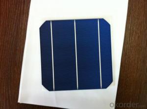


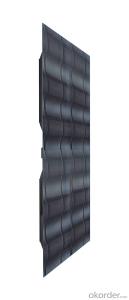
Solar Cell High Quality A Grade Cell Poly/Monocrystalline 5v
- Ref Price:
-

- Loading Port:
- Shanghai
- Payment Terms:
- TT OR LC
- Min Order Qty:
- 1000 pc
- Supply Capability:
- 100000 pc/month
OKorder Service Pledge
OKorder Financial Service
You Might Also Like


Specifications
hot sale solar cell
1.16.8%~18.25% high efficiency
2.100% checked quality
3.ISO9001/ISO14001/TUV/CE/UL
4.stable performance
We can offer you the best quality products and services, don't miss !
POLY6'(156*156)
Polycrystalline Silicon Solar cell
Physical Characteristics
Dimension: 156mm×156mm±0.5mm
Diagonal: 220mm±0.5mm
Thickness(Si): 200±20 μm
Front(-) Back(+)
Blue anti-reflecting coating (silicon nitride); Aluminum back surface field;
1.5mm wide bus bars; 2.0mm wide soldering pads;
Distance between bus bars: 51mm . Distance between bus bars :51mm .
Electrical Characteristics
Efficiency(%) | 18.00 | 17.80 | 17.60 | 17.40 | 17.20 | 16.80 | 16.60 | 16.40 | 16.20 | 16.00 | 15.80 | 15.60 |
Pmpp(W) | 4.33 | 4.29 | 4.24 | 4.19 | 4.14 | 4.09 | 4.04 | 3.99 | 3.94 | 3.90 | 3.86 | 3.82 |
Umpp(V) | 0.530 | 0.527 | 0.524 | 0.521 | 0.518 | 0.516 | 0.514 | 0.511 | 0.509 | 0.506 | 0.503 | 0.501 |
Impp(A) | 8.159 | 8.126 | 8.081 | 8.035 | 7.990 | 7.938 | 7.876 | 7.813 | 7.754 | 7.698 | 7.642 | 7.586 |
Uoc(V) | 0.633 | 0.631 | 0.628 | 0.625 | 0.623 | 0.620 | 0.618 | 0.617 | 0.615 | 0.613 | 0.611 | 0.609 |
Isc(A) | 8.709 | 8.677 | 8.629 | 8.578 | 8.531 | 8.478 | 8.419 | 8.356 | 8.289 | 8.220 | 8.151 | 8.083 |

MONO5'(125*125mm)165
Monocrystalline silicon solar cell
Physical Characteristics
Dimension: 125mm×125mm±0.5mm
Diagonal: 165mm±0.5mm
Thickness(Si): 200±20 μm
Front(-) Back(+)
Blue anti-reflecting coating(silicon nitride); Aluminum back surface field;
1.6mmwide bus bars; 2.5mm wide soldering pads;
Distance between bus bars: 61mm . Distance between bus bars :61mm .
Electrical Characteristics
Efficiency(%) | 19.40 | 19.20 | 19.00 | 18.80 | 18.60 | 18.40 | 18.20 | 18.00 | 17.80 | 17.60 | 17.40 | 17.20 |
Pmpp(W) | 2.97 | 2.94 | 2.91 | 2.88 | 2.85 | 2.82 | 2.79 | 2.76 | 2.73 | 2.70 | 2.67 | 2.62 |
Umpp(V) | 0.537 | 0.535 | 0.533 | 0.531 | 0.527 | 0.524 | 0.521 | 0.518 | 0.516 | 0.515 | 0.513 | 0.509 |
Impp(A) | 5.531 | 5.495 | 5.460 | 5.424 | 5.408 | 5.382 | 5.355 | 5.328 | 5.291 | 5.243 | 5.195 | 4.147 |
Uoc(V) | 0.637 | 0.637 | 0.636 | 0.635 | 0.633 | 0.630 | 0.629 | 0.629 | 0.628 | 0.626 | 0.626 | 0.625 |
Isc(A) | 5.888 | 5.876 | 5.862 | 5.848 | 5.839 | 5.826 | 5.809 | 5.791 | 5.779 | 5.756 | 5.293 | 5.144 |

FAQ:
Q:How can i get some sample?
A:Yes , if you want order ,sample is not a problem.
Q:How about your solar panel efficency?
A: Our product efficency around 17.25%~18.25%.
Q:What’s the certificate you have got?
A: we have overall product certificate of ISO9001/ISO14001/CE/TUV/UL
- Q:What is the role of a mounting structure in a solar silicon wafer?
- The role of a mounting structure in a solar silicon wafer is to provide support and stability to the wafer, allowing it to be securely attached to the solar panel or module. This structure ensures that the wafer remains in the correct position and orientation for optimal absorption of sunlight, maximizing the efficiency of the solar cell. It also helps protect the wafer from external forces such as wind, rain, and vibrations, ensuring its longevity and reliable performance.
- Q:How are solar silicon wafers protected from thermal damage?
- Solar silicon wafers are protected from thermal damage through the implementation of various techniques. One common method is the use of anti-reflective coatings on the surface of the wafers, which helps to reduce the absorption of heat and minimize thermal stress. Additionally, some wafers are equipped with backside passivation layers that enhance their ability to dissipate heat. Moreover, proper packaging and installation of solar panels also play a crucial role in safeguarding the wafers from thermal damage by ensuring adequate heat dissipation and temperature control.
- Q:How does the efficiency of a solar silicon wafer vary with different angles of sunlight?
- The efficiency of a solar silicon wafer generally varies with different angles of sunlight. It is highest when sunlight falls perpendicularly onto the wafer, maximizing the absorption of solar energy and resulting in optimal conversion to electricity. As the angle of sunlight deviates from perpendicular, the efficiency gradually decreases due to increased reflection and decreased absorption of light. However, modern solar technologies and tracking systems are designed to optimize the angle of sunlight incidence, allowing for better efficiency even at non-perpendicular angles.
- Q:What are the challenges in recycling solar silicon wafers?
- One of the main challenges in recycling solar silicon wafers is the complex and costly process involved in recovering the valuable materials from the wafers. The wafers are typically made of high-purity silicon, which requires specialized techniques to separate and purify. Additionally, the wafers are often coated with various layers of metals and other materials, making the recycling process more complicated. Furthermore, the collection and sorting of used wafers from various sources can be challenging, as they are typically small and lightweight. Overall, the challenges in recycling solar silicon wafers lie in the intricate recovery process, the complexity of the materials used, and the logistics of collection and sorting.
- Q:The raw material of the solar cell is the silicon chip, some manufacturers specialize in the production of monocrystalline silicon, polycrystalline silicon chip, the production of monocrystalline silicon, polycrystalline silicon chip, what is the use of raw materials? Also ask how much raw material costs in recent years? Thank you!!
- Polysilicon material:1 solar polysilicon: 6N, P2 head tails: P3 broken semiconductor wafer: P type, arc type debrisPrice: $200 / kg
- Q:Process flow of wafer wafer ultrasonic cleaning machine?
- Plasma cleaning relates to the field of etching technology, and fully satisfies the removal of residual surface of silicon wafer after etching processKeep particle cleaningBackground technologyIn the etching process, the particles come from many sources: etching gas such as Cl2, HBr, CF4 etc. are corrosive, etching after the end will have a certain number of particles on the surface of the silicon wafer reaction chamber; a quartz cover will produce quartz particles in plasma bombardment; reaction chamber liner (liner) also metal particles will be produced in the etching process for long time. The surface residual silicon etching after particles block conductive connection, cause damage to the device. Therefore, the control of particles is very important in the etching process.
- Q:Can solar silicon wafers be used in water desalination systems?
- Yes, solar silicon wafers can be used in water desalination systems. These wafers can be utilized to generate electricity through photovoltaic cells, which can then power the desalination process. This approach, known as solar-powered desalination, offers a sustainable and environmentally-friendly solution to convert saltwater into freshwater using solar energy.
- Q:How are solar silicon wafers tested for thermal properties?
- Solar silicon wafers are tested for thermal properties through various methods such as thermal conductivity measurements, thermoreflectance imaging, and infrared thermography. These techniques allow the determination of the wafer's ability to conduct heat efficiently, detect any defects or irregularities, and assess its overall thermal performance.
- Q:Are solar silicon wafers affected by shading?
- Yes, solar silicon wafers are affected by shading. Shading can significantly reduce the efficiency and power output of solar panels as shaded areas on the silicon wafers block sunlight, leading to decreased electricity generation.
- Q:Are solar silicon wafers susceptible to cracking?
- Yes, solar silicon wafers are susceptible to cracking.
1. Manufacturer Overview |
|
|---|---|
| Location | |
| Year Established | |
| Annual Output Value | |
| Main Markets | |
| Company Certifications | |
2. Manufacturer Certificates |
|
|---|---|
| a) Certification Name | |
| Range | |
| Reference | |
| Validity Period | |
3. Manufacturer Capability |
|
|---|---|
| a)Trade Capacity | |
| Nearest Port | |
| Export Percentage | |
| No.of Employees in Trade Department | |
| Language Spoken: | |
| b)Factory Information | |
| Factory Size: | |
| No. of Production Lines | |
| Contract Manufacturing | |
| Product Price Range | |
Send your message to us
Solar Cell High Quality A Grade Cell Poly/Monocrystalline 5v
- Ref Price:
-
- Loading Port:
- Shanghai
- Payment Terms:
- TT OR LC
- Min Order Qty:
- 1000 pc
- Supply Capability:
- 100000 pc/month
OKorder Service Pledge
OKorder Financial Service
Similar products


New products
Hot products


Hot Searches
Related keywords